

Testing method for guiding hole coppering thickness in wiring board
A test method and via hole technology are applied in the field of measuring copper plating thickness of via holes in flexible circuit boards on production lines, which can solve problems such as damage to products and waste.
Active Publication Date: 2009-03-18
靖江德方科技服务有限公司
View PDF5 Cites 0 Cited by
- Summary
- Abstract
- Description
- Claims
- Application Information
AI Technical Summary
Problems solved by technology
However, this method of testing the copper plating thickness of the via hole will destroy the product and cause a certain degree of waste.
Method used
View moreImage
Smart ImageViewing Examples

Examples
Embodiment 2
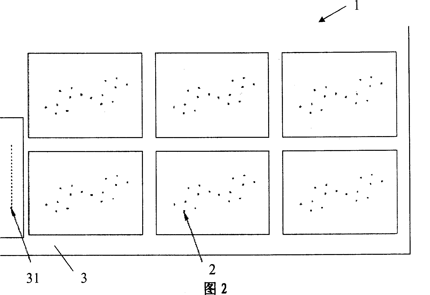
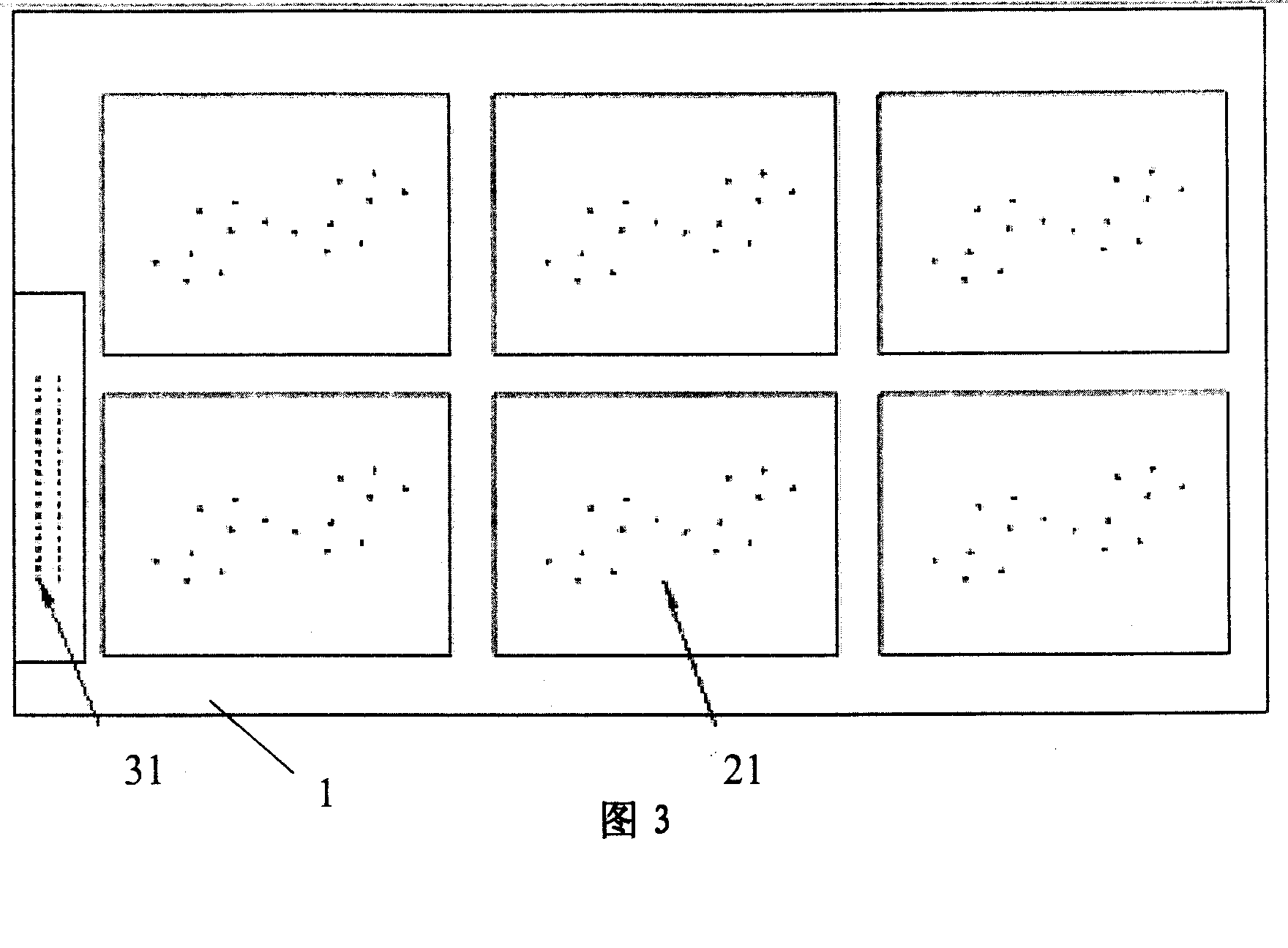
[0021] In a four-layer flexible printed circuit board product, the size of the via hole in the product is 0.25mm and 0.3mm. The specific implementation method is as follows: firstly, when drilling holes after cutting the copper foil, 20 0.25mm and 20 0.3mm two kinds of drilling holes are added in the scrap copper area, and the arrangement is shown in Figure 3. Copper plating is carried out by the hole plating process. After the copper plating is completed, it is cut off, and the hole section is analyzed, and the thickness of the hole copper is measured on a metallographic microscope (Jenco Instruments Inc. Model MET-233). The test results are listed in Table 2.
Login to View More PUM
 Abstract
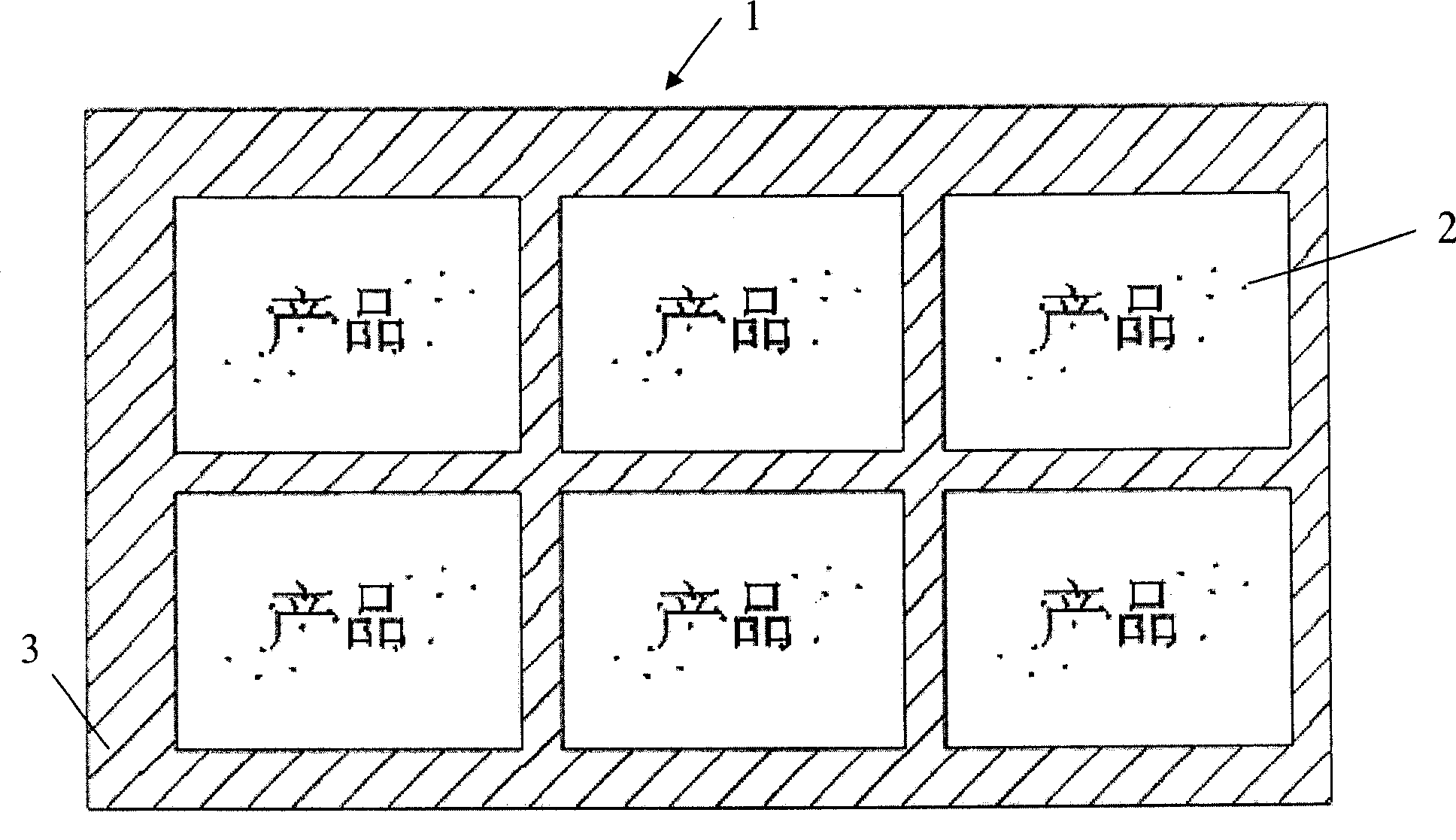
A testing method for the coppering thickness of onstate hole in the wiring board is disclosed that includes following steps: A. when designing the composing mode of the wiring board, a row or several rows of holes which have same size with the onstate holes in the flexible wiring board productions are drilled on the waste copper area beside the production; B. after the electric plating, the samples of the onstate holes are cut form the waste copper area, and the cross sections are abraded, burnished and eroded; the thickness of the cross section of the cover is measured. A composing mode which is convenient for measuring the thickness of testing holes is adopted in the invention, and it can measure the coppering thickness of onstate holes precisely and effectively without destroying the production.
Description
【Technical field】 [0001] The invention relates to a method for measuring the copper plating thickness of the through hole of the circuit board, in particular to a method for measuring the copper plating thickness of the through hole in the flexible circuit board on the production line. 【Background technique】 [0002] For the copper plating thickness of the via hole of the circuit board, it is usually measured by a microscope measurement method. The specific method is: after the copper plating is completed, cut a few products from the layout, put them into the liquid epoxy resin, add a catalyst, and cure After solidification, the cross-section is properly ground, polished and etched, and the thickness of the cross-section of the covering layer is measured with a corrected ruler on a metallographic microscope. Among them, the purpose of grinding and polishing is to make the surface of the cross-section smooth, generally it is enough to grind until the cross-section of the thro...
Claims
Login to View More Application Information
Patent Timeline
 Patent Type & AuthorityPatents(China)
IPC IPC(8): G01B11/06G01B21/08
Inventor张世平
Owner靖江德方科技服务有限公司