Stack type chip package with radiation structure

A chip and multi-chip technology, applied in the field of multi-chip offset stacked package structure, can solve the problems of the limitation of the number of chip stacks and the inability to further reduce the thickness of the stacked chip package structure 100

Active Publication Date: 2009-06-24
CHIPMOS TECH INC
View PDF3 Cites 0 Cited by
  • Summary
  • Abstract
  • Description
  • Claims
  • Application Information

AI Technical Summary

Problems solved by technology

However, when the known technology stacks a plurality of chips of different sizes into the stacked chip package structure 10 in the above-mentioned manner, since the size of the chip on the upper layer must be smaller, the stacked chip package structure 10 has the number of stacked chips. limit
[0007] In the above two stacking methods, Figure 1A The method of using the spacer 130 is likely to cause the disadvantage that the thickness of the stacked chip packaging structure 100 cannot be further reduced; and Figure 1B , since the chip size of the upper layer must be smaller, this will cause the problem that the design or use of the chip will be limited

Method used


Image

  • Stack type chip package with radiation structure
  • Stack type chip package with radiation structure
  • Stack type chip package with radiation structure

Examples


Embodiment approach

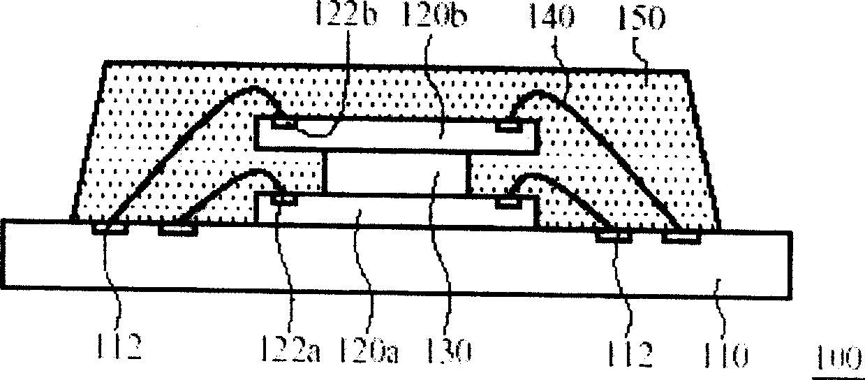
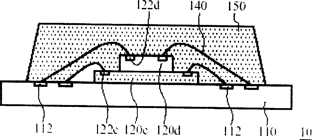
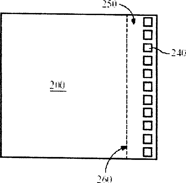
[0074] as reference Figure 2A and Figure 2B As shown, a schematic plan view and a schematic cross-sectional view of the chip 200 that has completed the aforementioned process. Such as Figure 2A As shown, the chip 200 has an active surface 210 and a back surface 220 opposite to the active surface, and an adhesive layer 230 has been formed on the chip back surface 220; it should be emphasized here that the adhesive layer 230 of the present invention is not limited to the aforementioned semi-cured glue. The purpose of the adhesive layer 230 is to form a bond with the substrate or the chip. Therefore, as long as it is an adhesive material with this function, it is an embodiment of the present invention, such as a die attached film. In addition, in the embodiment of the present invention, a plurality of bonding pads 240 are disposed on the active surface 210 of the chip 200, and the plurality of bonding pads 240 have been disposed on the side of the chip 200, therefore, the wi...


PUM


Abstract

The invention discloses a stack package structure with a confluence frame on a lead frame, which includes: a lead frame, a plurality of inner pin groups and outer pin groups arranged face to face and a chip holder, wherein, the chip holder is arranged among the inner pin groups and a height difference is formed between the chip holder and the inner pin groups; at least a confluence frame with an upper surface and a lower surface is positioned between the inner draw feet groups and the chip holder; a multi-chip offset stack structure is formed by the stack of a plurality of chips. The multi-chip offset stack structure is fixedly connected with the a first surface of the chip holder and is electrically connected with the plurality of inner pin groups; and an package body coats the multi-chip offset stack structure, the inner pin groups, the first surface of the chip holder and the upper surface of the confluence frame, and exposes a second surface of the chip holder and the lower surface of the confluence frame and juts the plurality of outer pin groups out of the package body.

Description

technical field [0001] The invention relates to a multi-chip offset stack package structure, in particular to a multi-chip offset stack package with a heat dissipation structure. Background technique [0002] In recent years, three-dimensional (3D) packaging is being carried out in the back-end process of semiconductors, in order to use the least area to achieve relatively large semiconductor integration (Integrated) or memory capacity. In order to achieve this goal, a three-dimensional (Three Dimension; 3D) package has been developed using a chip stacked method. [0003] In the known technology, chips are stacked in such a way that multiple chips are stacked on a substrate, and then a wire bonding process is used to connect the multiple chips to the substrate. Figure 1A It is a schematic cross-sectional view of a known stacked chip package structure with the same or similar chip size. Such as Figure 1A As shown, the known stacked chip package structure 10 , 100 includes ...

Claims


Application Information

Patent Timeline
Patent Type & Authority Patents(China)
IPC IPC(8): H01L25/00H01L25/065H01L25/18H01L23/488H01L23/495H01L23/34H01L23/31
CPCH01L2224/32245H01L2924/19107H01L2224/73265H01L2224/48247H01L2224/32145H01L2225/06562H01L2224/48145H01L2224/4911H01L2924/181H01L2224/48147H01L2224/023H01L2924/00H01L2924/00012H01L2924/0001
Inventor 陈煜仁沈更新林鸿村
Owner CHIPMOS TECH INC
Why Eureka
Try Eureka