3D chip packaging structure and preparation method thereof

A chip packaging structure, 3D technology, applied in semiconductor/solid-state device manufacturing, electrical components, electric solid-state devices, etc., can solve the problems of inability to meet the development trend of miniaturization, insufficient integration, high cost, etc., to meet the miniaturization development The needs of the trend, the effect of high packaging integration and low cost

Pending Publication Date: 2020-12-08
SJ SEMICON JIANGYIN CORP
View PDF0 Cites 0 Cited by
  • Summary
  • Abstract
  • Description
  • Claims
  • Application Information

AI Technical Summary

Problems solved by technology

[0004] In view of the shortcomings of the prior art described above, the purpose of the present invention is to provide a 3D chip packaging structure and its preparation method, which are used to solve the problems of high cost, insufficient integration, and low The problem of not being able to meet the needs of the development trend of miniaturization

Method used


Image

  • 3D chip packaging structure and preparation method thereof
  • 3D chip packaging structure and preparation method thereof
  • 3D chip packaging structure and preparation method thereof

Examples


Embodiment 1

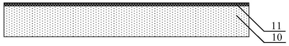
[0080] see figure 1 , the present invention provides a method for preparing a 3D chip packaging structure, the method for preparing the 3D chip packaging structure includes the following steps:

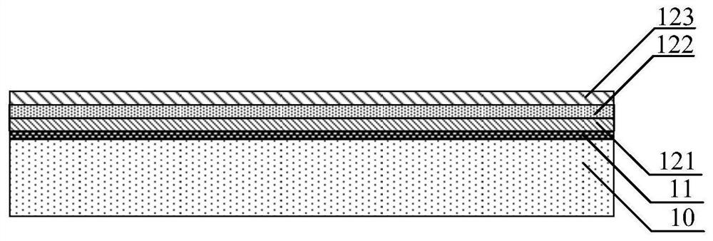
[0081] 1) providing a base, and forming a sacrificial layer on the upper surface of the base;

[0082] 2) forming a rewiring layer on the upper surface of the sacrificial layer;

[0083] 3) providing a chip, flip-chip bonding the chip to the upper surface of the rewiring layer, and electrically connecting the chip to the rewiring layer;

[0084] 4) Forming a first electrical connection structure and a first plastic encapsulation layer on the upper surface of the rewiring layer; the first electrical connection structure is located in the first plastic encapsulation layer, and the first electrical connection structure and the redistribution layer The wiring layer is electrically connected; the first plastic sealing layer plastic-seals the chip and the first electrical connection struc...

Embodiment 2

[0147] Please combine Figure 2 to Figure 17 read on Figure 18 , the present invention also provides a 3D chip packaging structure, the 3D chip packaging structure includes: a rewiring layer 12; a chip 13, the chip 13 is flip-chip bonded to the upper surface of the rewiring layer 12, and the The chip 13 is electrically connected to the rewiring layer 12; the first electrical connection structure 14, the first electrical connection structure 14 is located on the upper surface of the rewiring layer 12, and the first electrical connection structure 14 is connected to the The rewiring layer 12 is electrically connected; the first plastic sealing layer 15, the first plastic sealing layer 15 is located on the upper surface of the rewiring layer 12, and the first plastic sealing layer 15 connects the chip 13 and the first electrical The connection structure 14 is plastic-encapsulated; the second electrical connection structure 18, the second electrical connection structure 18 is lo...


PUM


Abstract

The invention provides a 3D chip packaging structure and a preparation method thereof. The 3D chip packaging structure comprises: a rewiring layer; a chip which is bonded on the upper surface of the rewiring layer in a flip-chip manner; a first electric connection structure which is located on the upper surface of the rewiring layer; a first plastic package layer which is positioned on the upper surface of the rewiring layer and is used for carrying out plastic package on the chip and the first electric connection structure; a second electric connection structure which is located on the uppersurface of the first plastic package layer; a second plastic package layer which is located on the upper surface of the first plastic package layer; a third electric connection structure which is located on the upper surface of the second plastic package layer; a third plastic package layer which is positioned on the upper surface of the second plastic package layer and is used for carrying out plastic package on the third electric connection structure; a top metal wire layer which is positioned on the upper surface of the third plastic package layer; and a solder ball bump located on the lower surface of the redistribution layer. According to the 3D chip packaging structure, 3D packaging of the chip is achieved, the cost is low, the packaging integration degree is high, and the requirement for the miniaturization development trend can be met.

Description

technical field [0001] The invention relates to the technical field of semiconductor packaging, in particular to a 3D chip packaging structure and a preparation method thereof. Background technique [0002] Lower cost, more reliable, faster and higher density circuits are the goals pursued by integrated circuit packaging. In the future, integrated circuit packaging will increase the integration density of various electronic components by continuously reducing the minimum feature size. Currently, advanced packaging methods include: Wafer Level Chip Scale Packaging (WLCSP), Fan-Out Wafer Level Package (FOWLP), Flip Chip, Package on Package (Package on Package, POP) and so on. [0003] However, the existing above-mentioned packaging methods and the packaging structures obtained by the above-mentioned packaging methods all have the problems of high cost, insufficient integration, and inability to meet the needs of the development trend of miniaturization. Contents of the inv...

Claims


Application Information

Patent Timeline
Patent Type & Authority Applications(China)
IPC IPC(8): H01L21/56H01L23/31H01L23/498
CPCH01L21/568H01L23/3128H01L23/3135H01L23/49816H01L23/49827H01L23/49838H01L2224/16225H01L2924/181H01L2924/00012
Inventor 吴政达吕娇陈彦亨林正忠
Owner SJ SEMICON JIANGYIN CORP
Why Eureka
Try Eureka