Check patentability & draft patents in minutes with Patsnap Eureka AI!

A device and method to eliminate signal burr

A technology for eliminating signals and burrs, which is applied in the field of signal processing, can solve problems such as narrow adaptation surface, and achieve the effect of wide adaptation range

Inactive Publication Date: 2009-07-01
VIMICRO CORP
View PDF4 Cites 0 Cited by
  • Summary
  • Abstract
  • Description
  • Claims
  • Application Information

AI Technical Summary

Problems solved by technology

[0017] The main disadvantage of the above-mentioned deburring methods is that each method is only applicable to a specific application scenario, not a general deburring method, and the adaptability is narrow

Method used


Image

  • A device and method to eliminate signal burr
  • A device and method to eliminate signal burr
  • A device and method to eliminate signal burr

Examples


Embodiment Construction

[0045] The present invention will be further described in detail below in conjunction with the drawings and specific embodiments.

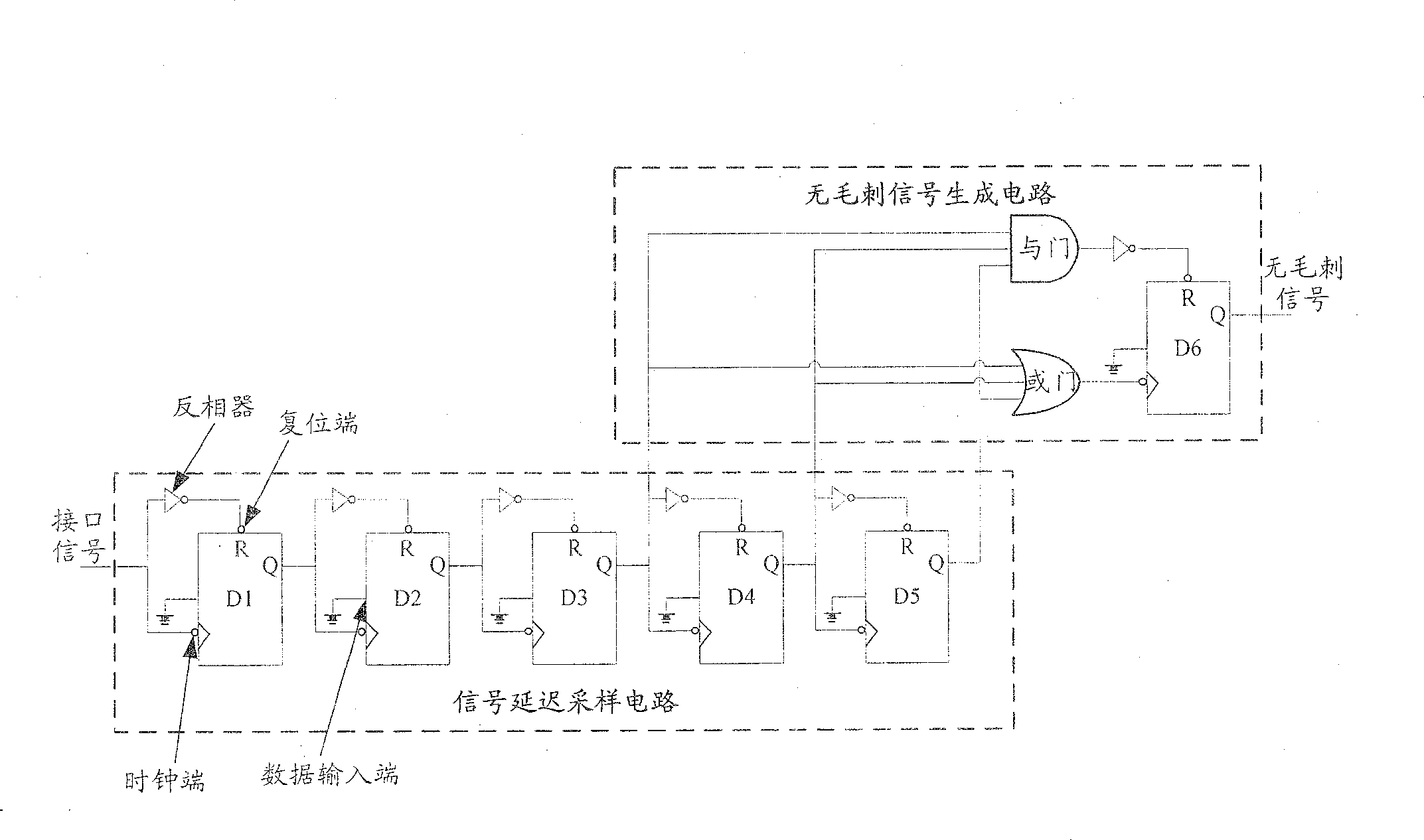
[0046] image 3 This is a diagram of an apparatus for eliminating glitches in a signal provided by an embodiment of the present invention, such as image 3 As shown, it mainly includes: signal delay sampling circuit and glitch-free signal generation circuit, among which:

[0047] Signal delay sampling circuit: used to perform N+m-level delay processing on the input interface signal to be removed from the burr. The delay time of the two adjacent stages is equal to Tclk-q, which will be obtained by the m+1~N+m-th stage delay processing The m+1~m+N-th stage delayed signal is output to the glitch-free signal generating circuit.

[0048] Here, Tclk-q is the length of time between the rising or falling edge of the clock end of the latch when the valid edge occurs to the time when the output of the latch changes; N is the maximum width of the glitch to be e...


PUM


Abstract

The invention discloses a device for eliminating signal burrs, which comprises: a signal delay sampling circuit and a burr-free signal generation circuit. The invention also discloses a method for eliminating signal burrs, which includes: determining the delay series according to the maximum width of the burr to be eliminated, and performing delay processing on the interface signal to be eliminated according to the delay series; Stage delay signals are respectively subjected to logical AND operation and logical OR operation, and a glitch-free signal is obtained according to the logical AND operation result and the logical OR operation result. The present invention can remove burrs generated in various ways, and has a wide range of applications.

Description

Technical field [0001] The present invention relates to the technical field of signal processing, in particular to a device and method for eliminating signal glitches. Background technique [0002] The advancement of semiconductor technology makes electronic systems work more and more frequently, and there are more and more radio frequency, analog and digital components integrated on the same platform or even system-on-chip (SoC). As a result, the interface signals of the chip are becoming more and more susceptible to interference, resulting in glitches. The so-called glitch is a signal whose width is less than the defined minimum width. How to eliminate glitches has become the most common problem in the design of chip interface modules. [0003] figure 1 Gives a schematic diagram of the process of burr generation, such as figure 1 As shown, the output signal of chip 1 passes through the output circuit of chip 1, the signal transmission line and the input circuit of chip 2 to ...

Claims


Application Information

Patent Timeline
Patent Type & Authority Patents(China)
IPC IPC(8): H03K5/00H03K5/1252G06F13/38
Inventor 马凤翔
Owner VIMICRO CORP
Features
  • R&D
  • Intellectual Property
  • Life Sciences
  • Materials
  • Tech Scout
  • Unparalleled Data Quality
  • Higher Quality Content
  • 60% Fewer Hallucinations
Learn More