CCD output node with single-hold structure

A technology of output node and hole structure, which is applied in the direction of electrical components, electric solid devices, circuits, etc., can solve the problems of occupying, increasing capacitance, reducing CCD charge packet conversion sensitivity, etc.

Inactive Publication Date: 2009-09-02
THE 44TH INST OF CHINA ELECTRONICS TECH GROUP CORP
View PDF3 Cites 0 Cited by
  • Summary
  • Abstract
  • Description
  • Claims
  • Application Information

AI Technical Summary

Problems solved by technology

The traditional structure is to open a contact hole at the output diode of the CCD, open a contact hole on the gate of the MOS transistor of the source follower amplifier, and connect the two contact holes with metal. Since there is a certain distance between the two contact holes, And the two contact holes also occupy a certain area, which increases the capacitance of this node and reduces the conversion sensitivity of the CCD charge packet. The unit of conversion sensitivity is: microvolts / electrons

Method used


Image

  • CCD output node with single-hold structure
  • CCD output node with single-hold structure
  • CCD output node with single-hold structure

Examples


Embodiment

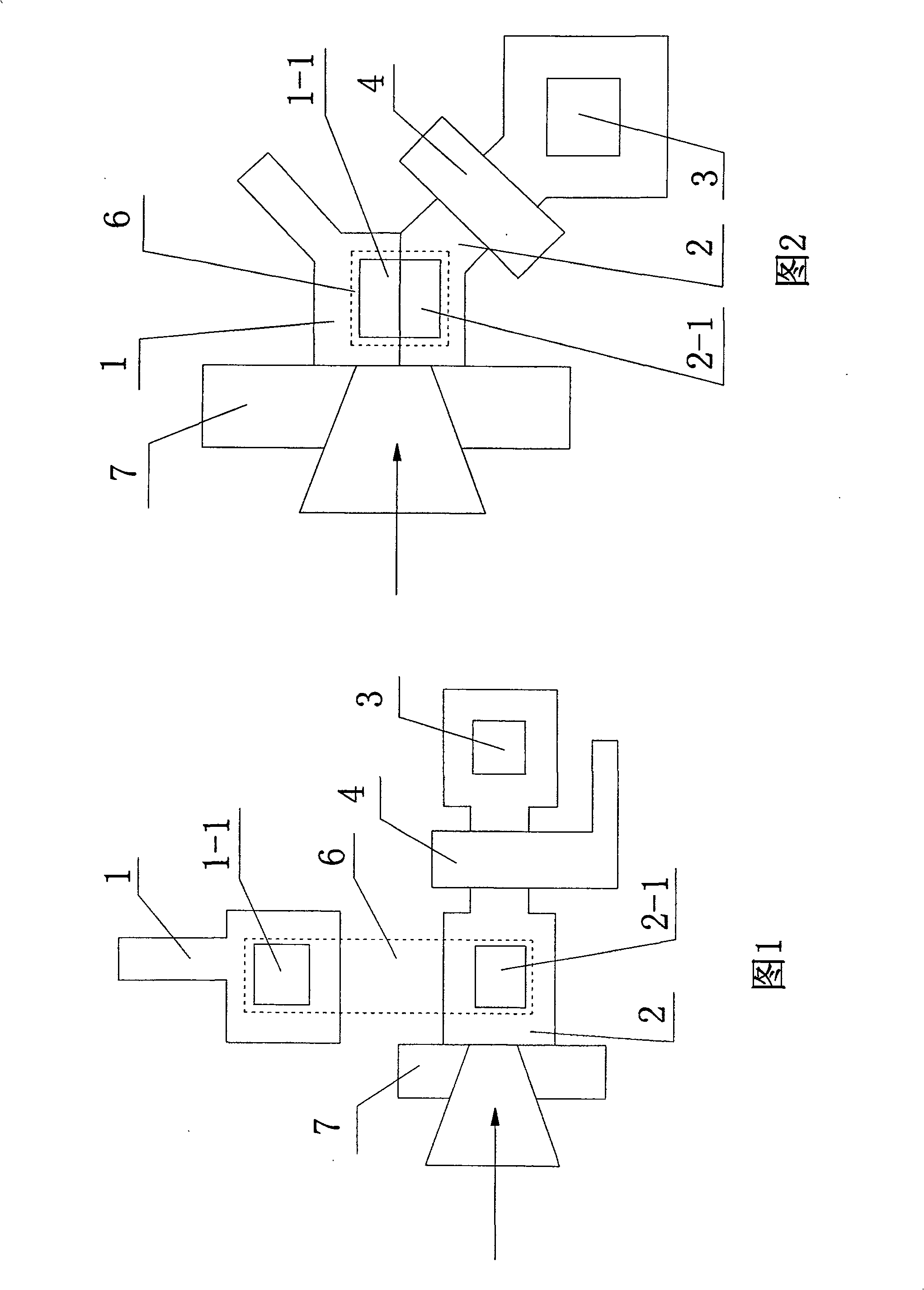
[0032] See attached figure 2 , a schematic diagram of the contact hole connection structure of the CCD output diode and the MOS tube grid of the present invention, a CCD output node with a single hole structure, which includes: MOS tube grid 1, MOS tube grid contact hole 1-1, CCD output diode 2, The CCD output diode contact hole 2-1, the drain 3 of the reset transistor and the gate 4 of the reset transistor are special in that: the MOS tube grid 1 and the CCD output diode 2 overlap, so that the MOS tube grid contact hole The distance between 1-1 and the CCD output diode contact hole 2-1 is zero; a metal is formed on the two contact holes, and the metal connects the MOS tube gate contact hole 1-1 and the CCD output diode contact hole 2-1.

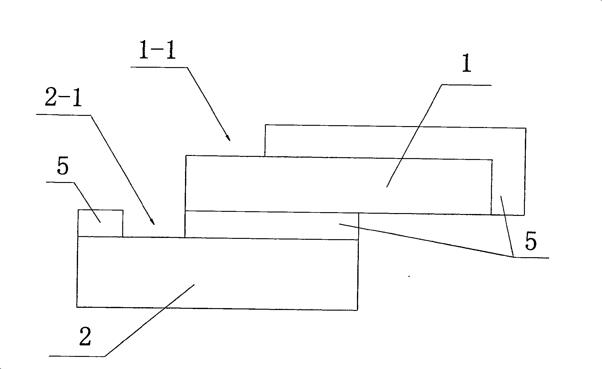
[0033] See attached image 3 , the contact hole position relationship diagram of CCD output diode and MOS tube grid of the present invention, as can be seen from the figure, MOS tube grid 1 overlaps with CCD output diode 2, and MOS tube gr...


PUM


Abstract

The invention discloses a CCD output node with a single-hole structure, which includes: MOS tube grid, MOS tube grid contact hole, CCD output diode, CCD output diode contact hole, reset drain and reset gate, and its special features are: the The MOS tube grid and the CCD output diode overlap, so that the distance between the MOS tube grid contact hole and the CCD output diode contact hole is zero, and a metal is formed on the two contact holes, and the metal is connected to the MOS tube grid contact hole and the CCD output diode. Contact hole; this structure can regard the two contact holes as a whole as a new contact hole, which solves the problem of corresponding capacitance due to a certain distance between the two contact holes; the beneficial technical effect of the present invention is: under the same conditions The CCD output amplitude is 15% higher than that of the conventional structure, and it can image the target under weaker light.

Description

technical field [0001] The invention relates to a charge coupled device, in particular to a CCD output node with a single hole structure. Background technique [0002] The signal charge packet of the charge-coupled device (CCD) needs to be amplified before being output off-chip, and the commonly used amplifier is a source-follower amplifier. The traditional structure is to open a contact hole at the output diode of the CCD, open a contact hole on the gate of the MOS transistor of the source follower amplifier, and connect the two contact holes with metal. Since there is a certain distance between the two contact holes, Moreover, the two contact holes also occupy a certain area, which increases the capacitance of this node and reduces the conversion sensitivity of the CCD charge packet. The unit of conversion sensitivity is microvolts / electron. [0003] The above is the structural mode and deficiency adopted by the CCD output node in the prior art. Based on this deficiency, ...

Claims


Application Information

Patent Timeline
Patent Type & Authority Patents(China)
IPC IPC(8): H01L27/02H01L27/06H01L23/522
Inventor 汪朝敏李仁豪
Owner THE 44TH INST OF CHINA ELECTRONICS TECH GROUP CORP
Why Eureka
Try Eureka