
Infrared receiver
A technology of infrared receivers and adhesives, applied in the field of infrared receivers, can solve problems such as the signal-to-noise ratio that is susceptible to interference, and achieve the goal of improving the signal-to-noise ratio, improving the anti-interference ability and signal-to-noise ratio, and increasing the output amplitude Effect
- Summary
- Abstract
- Description
- Claims
- Application Information
AI Technical Summary
Problems solved by technology
Method used
Image

Examples
Embodiment 1
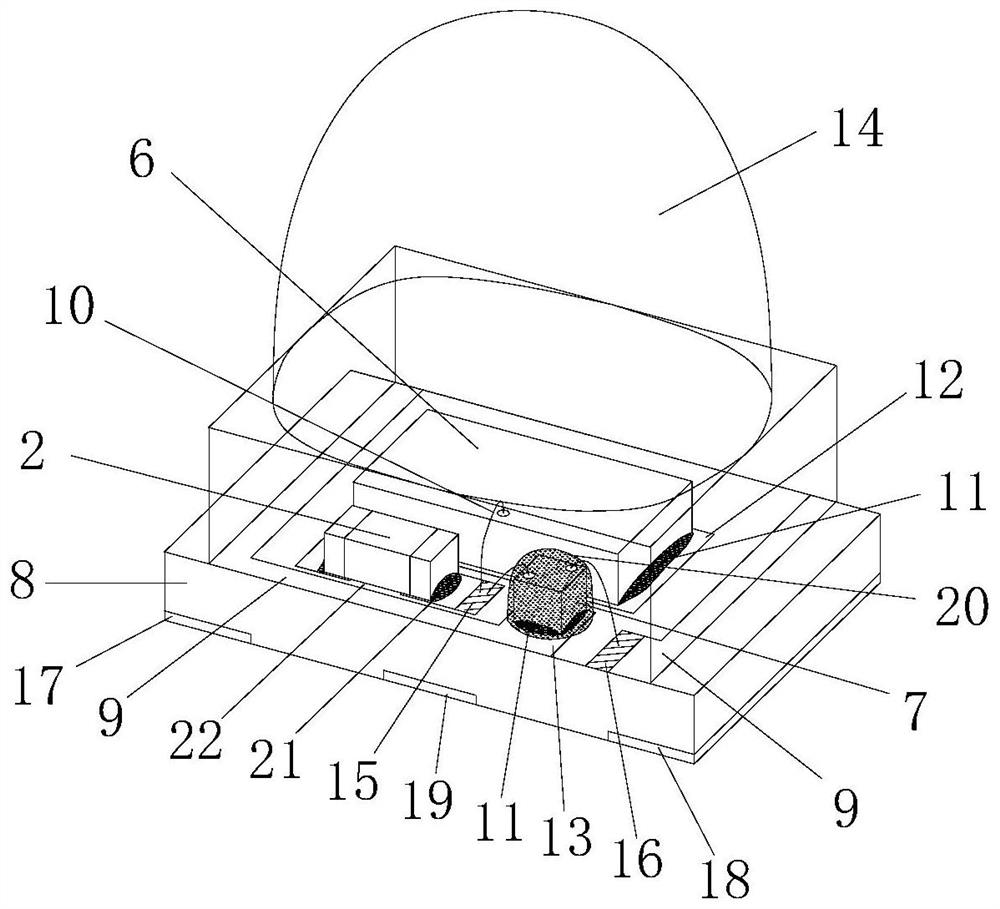
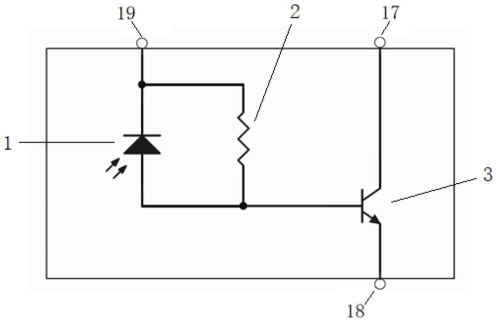
[0030] Such as figure 2 and image 3 As shown, the present embodiment provides an infrared receiver, which includes a photodiode chip 6, a triode chip 7 and a resistor 2, and also includes a substrate 8 and a package body 14. The package body 14 surrounds the top of the substrate 8, and the package body will be located on The photodiode chip 6, the triode chip 7 and the resistor 2 on the top of the substrate 8 are sealed together, the bottom of the substrate 8 is arranged outside the package body 14, and the bottom side of the substrate 8 is provided with a control pin 19, a collector pin 17 and an emission pin. Pole pin 18 and three external pins, photodiode chip 6 and triode chip 7 are electrically connected, resistor 2 is connected between the two electrodes of photodiode chip 6, and triode chip 7 is respectively connected to control pin 19, collector lead The pin 17 is electrically connected to the emitter pin 18 .
[0031] The substrate 8 is coated with a copper foil l...
Embodiment 2
[0044] Such as Figure 4 and Figure 5 As shown, the present embodiment adopts the lead frame 23 as the chip carrier, the photodiode chip 6, the triode chip 7 and the resistor 2 are fixed on the top of the lead frame 23, and the top of the lead frame 23 is also fixed with a PD base island for installing the photodiode 12. Install the TR base island 13 of the triode chip, the C bonding base island 24 and the D bonding base island 25 for bonding; the package body 14 surrounds the top of the lead frame 23, and the chips, base islands and bonding wires on the top are Seal together. The PD base island 12 extends outside the package body 14 to become the control pin 19, the TR base island 13 extends outside the package body 14 to become the collector pin 17, and the C bonding base The island 24 extends out of the package body 14 to become the emitter pin 18 .
[0045] The photodiode chip that can be used in this embodiment is a P substrate type photodiode chip or an N substrate t...
PUM
 Abstract
Description
Claims
Application Information