Wafer structure and forming method thereof
A wafer and ladder structure technology, applied in the manufacture of electrical components, electrical solid devices, semiconductor/solid devices, etc., can solve problems such as damage to electrical pad metal materials, brittle solder bumps, poor stacking, etc., to achieve improved Reliability, improved stackability, yield and quality effects
- Summary
- Abstract
- Description
- Claims
- Application Information
AI Technical Summary
Problems solved by technology
Method used
Image

Examples
no. 1 example
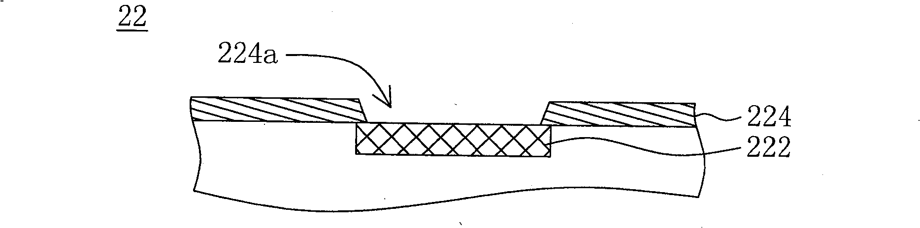
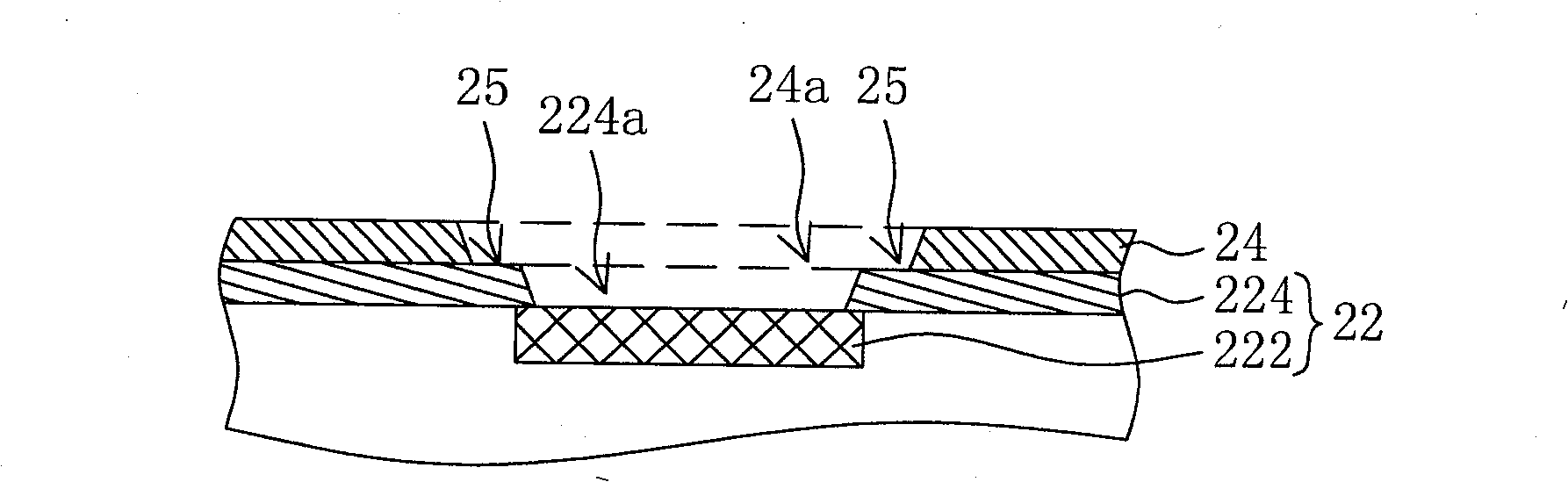
[0038] Please also refer to Figure 2A-2G , Figure 2A A schematic diagram illustrating a wafer according to a first embodiment of the present invention; Figure 2B shows that the second protective layer is formed on Figure 2A The schematic diagram on the first protective layer; Figure 2C Indicates that the adhesion layer is formed on Figure 2B The schematic diagram on the wafer and the second protective layer; Figure 2D The photoresist layer is shown formed in Figure 2C Schematic diagram on the adhesive layer of ; Figure 2E Shows barrier layer plating on Figure 2D Schematic diagram on the adhesive layer of ; Figure 2F Indicates that the wetting layer is formed in Figure 2E Schematic diagram on the barrier layer of ; Figure 2G draw Figure 2F Schematic diagram of removing the middle photoresist layer and part of the adhesive layer.
[0039] According to the method for forming a wafer structure according to the first embodiment of the present invention, a w...
no. 2 example
[0050] The difference between this embodiment and the above-mentioned first embodiment is that in this embodiment, a wetting layer is used to form a T-shaped or U-shaped plug. In addition, in the method for forming the wafer structure of this embodiment, the steps of providing a wafer, forming a second protective layer, forming an adhesive layer, and forming a photoresist layer are performed in the same manner at first, and these steps are the same as those of the first embodiment (such as Figure 2A-2D shown), and will not be repeated here.
[0051] Please also refer to Figure 4A and 4B , Figure 4A A schematic diagram showing the formation of the barrier layer on the adhesive layer according to the second embodiment of the present invention; Figure 4B Indicates that the wetting layer is formed in Figure 4A Schematic diagram of the barrier layer. The forming method of this embodiment is followed by a step of electroplating a barrier layer. Such as Figure 4A As show...
no. 3 example
[0057] The difference between this embodiment and the above-mentioned first embodiment mainly lies in the configuration of the photoresist layer and the method of forming the UBM layer, and the rest of the similarities will be omitted for brevity. Please also refer to Figures 6A-6G , Figure 6A A schematic diagram showing a wafer and a second protective layer according to a third embodiment of the present invention; Figure 6B Indicates that the adhesion layer is formed on Figure 6A The schematic diagram on the wafer and the second protective layer; Figure 6C shows that the barrier layer is formed in Figure 6B Schematic diagram on the adhesive layer of ; Figure 6D Indicates that the wetting layer is formed in Figure 6C Schematic diagram on the barrier layer of ; Figure 6E The photoresist layer is shown formed in Figure 6D Schematic diagram on the wetting layer of ; Figure 6F Draw to remove Figure 6E Schematic diagram of the wetting layer, barrier layer, and ...
PUM
 Abstract
Description
Claims
Application Information
 - R&D
- Intellectual Property
- Life Sciences
- Materials
- Tech Scout
- Unparalleled Data Quality
- Higher Quality Content
- 60% Fewer Hallucinations
Browse by: Latest US Patents, China's latest patents, Technical Efficacy Thesaurus, Application Domain, Technology Topic, Popular Technical Reports.
© 2025 PatSnap. All rights reserved.Legal|Privacy policy|Modern Slavery Act Transparency Statement|Sitemap|About US| Contact US: help@patsnap.com