
Bearing apparatus and its manufacture method, bearing table apparatus, and exposure apparatus

A technology of a supporting device and a manufacturing method, which can be applied to photolithography exposure devices, microlithography exposure equipment, semiconductor/solid-state device manufacturing, etc., can solve the problems of increasing the volume of air springs, incapable of applying vibration-proof devices, and low rigidity. , to achieve the effect of preventing deformation and preventing large-scale

Inactive Publication Date: 2009-12-02
NIKON CORP
View PDF6 Cites 2 Cited by
  • Summary
  • Abstract
  • Description
  • Claims
  • Application Information

AI Technical Summary

Problems solved by technology

Regarding vibration suppression, the lower the rigidity of the air spring, the better. However, since the rigidity of the air spring is inversely proportional to the volume, a large volume is required to obtain a low rigidity air spring.
Therefore, it has been considered to increase the volume of the internal space of the air bracket, or to attach an air container to the air bracket, but in either case, it is directly related to the enlargement of the device. Due to the limitation of the projected area (installation area) of the device, Ensuring large volumes is difficult
[0010] In particular, in recent years, the demand for miniaturization of semiconductor elements and high-speed exposure processing has been increasing. In order to respond to such demands, various vibrations from the ground of the factory where the exposure equipment is installed and accompanying vibrations in the exposure equipment have been studied. The vibration of the movement of the stage is not transmitted to the projection lens. However, as mentioned above, due to the limitation of the space in the exposure device, there is a limit to increase the volume of the air spring, and it may not be able to meet the increasingly strict exposure requirements in the future. Concerns about the vibration isolation performance of the device
[0011] Moreover, the anti-vibration device described in Japanese Patent Laid-Open No. Hei 5-340444 published earlier cannot be applied to precision devices such as exposure devices as it is. middle

Method used


Image

  • Bearing apparatus and its manufacture method, bearing table apparatus, and exposure apparatus
  • Bearing apparatus and its manufacture method, bearing table apparatus, and exposure apparatus
  • Bearing apparatus and its manufacture method, bearing table apparatus, and exposure apparatus

Examples


Embodiment Construction

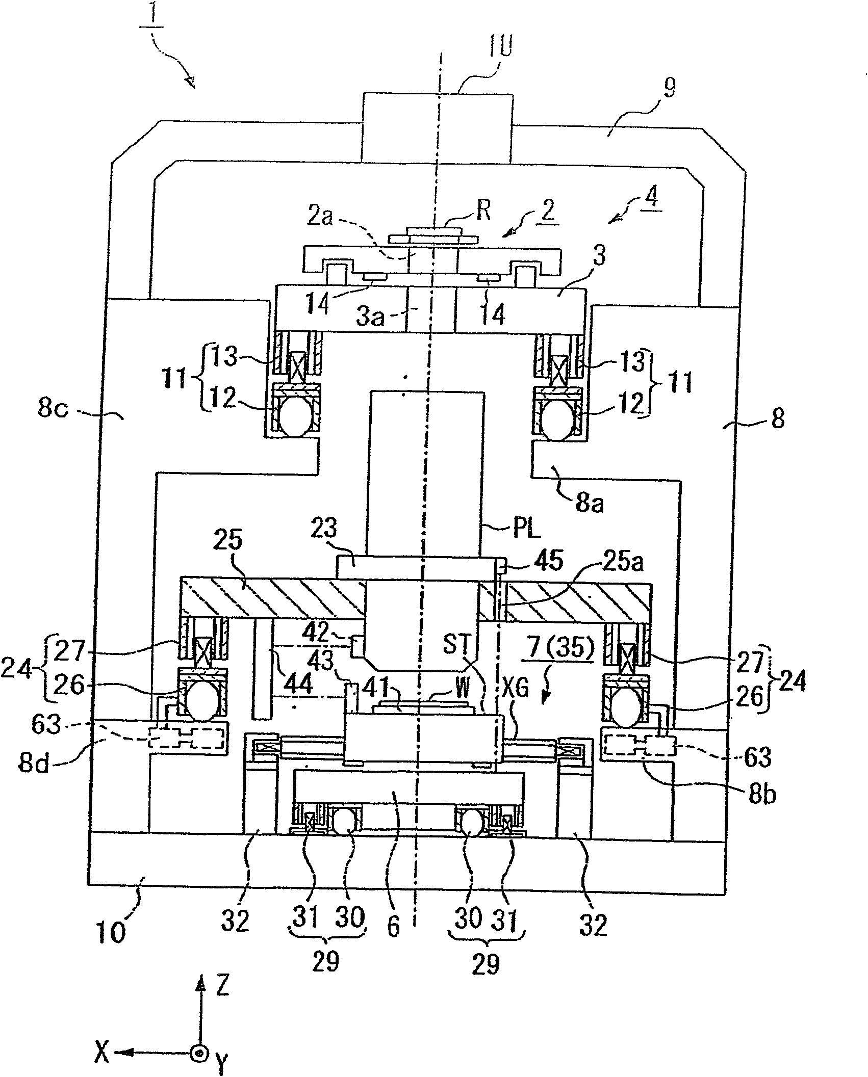
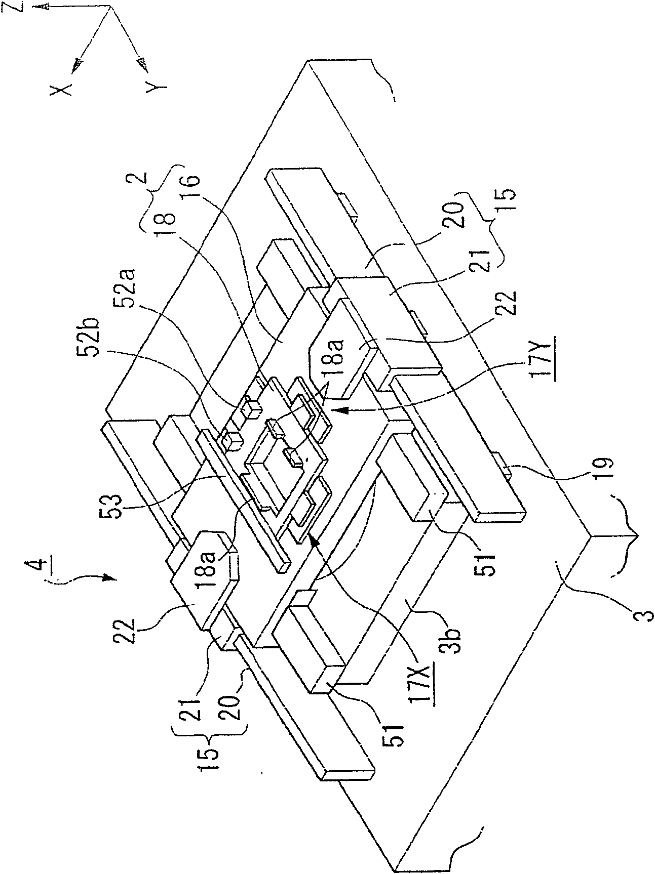
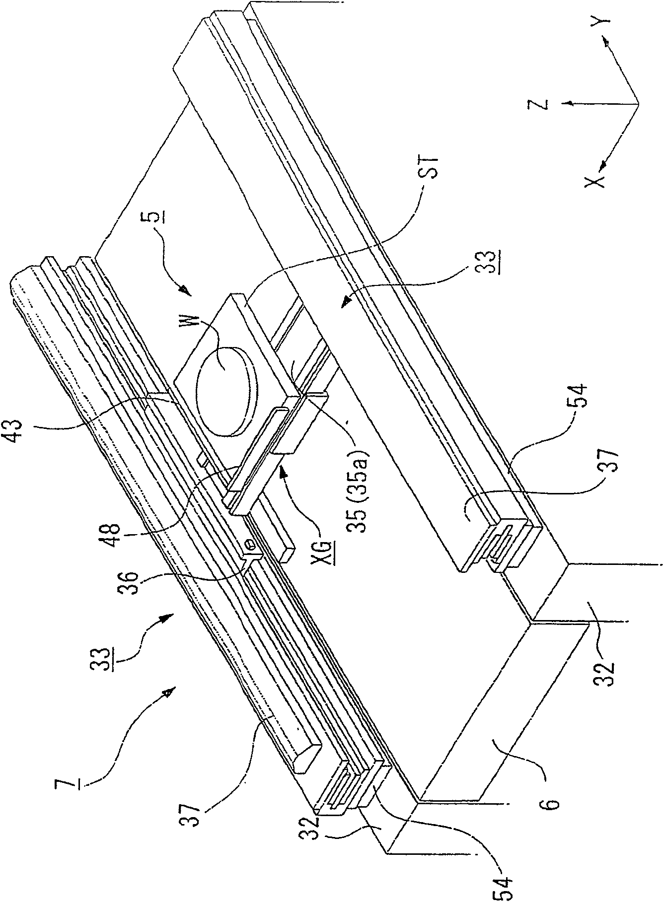
[0142] Refer to the following Figure 1 to Figure 14 Embodiments of the support device and its manufacturing method, stage device, and exposure device of the present invention will be described.

[0143]For example, an exposure apparatus will be described using an example in which a scanning type sequential exposure apparatus is used to transfer a circuit pattern of a semiconductor element formed on the reticle to a wafer while moving the reticle in synchronization with the wafer. Also, in this exposure apparatus, the supporting device of the present invention is applied to support the anti-vibration member of the projection optical system via the barrel platen. In these diagrams, pairs and shown as conventional examples Figure 15 The same constituent elements are assigned the same symbols and descriptions thereof are omitted.

[0144] figure 1 The exposure device shown is roughly composed of an illumination optical system IU that illuminates a rectangular (or arc-shaped) ...


PUM


Abstract

It includes a first gas chamber (61) that is filled with gas of a predetermined pressure and uses the gas to support the object PL, a support frame (8d) that supports the first gas chamber (61), and has a The second gas chamber (63) connected to the gas chamber (61) can function as a low-rigidity air spring without increasing the size of the device.

Description

technical field [0001] The present invention relates to a support device in which a gas chamber of a support object is supported by a support frame, a manufacturing method thereof, a stage device, and an exposure device used in the manufacture of semiconductor integrated circuits, liquid crystal displays, and the like. Background technique [0002] For a long time, in the etching process, which is one of the manufacturing processes of semiconductor elements, various methods are used to transfer the circuit pattern formed on the mask or grating (hereinafter referred to as grating) to the wafer coated with photoresist (photosensitive agent). Or an exposure device on a substrate such as a glass plate. [0003] For example, as an exposure device for semiconductor elements, for the miniaturization of the minimum line width (element rule) of the pattern accompanying the high integration of integrated circuits in recent years, it is mainly used to transfer the pattern of the gratin...

Claims


Application Information

Patent Timeline
Patent Type & Authority Patents(China)
IPC IPC(8): H01L21/027H01L21/68G03F7/20F16F15/04
CPCG03F7/709H01L21/682G03F7/70833H01L21/027
Inventor 高桥正人山本幸治
Owner NIKON CORP
Learn More