

Memory bus termination
Patent Information
- Authority / Receiving Office
- CN · China
- Current Assignee / Owner
- INTEL CORP
- Publication Date
- 2010-01-20
- Estimated Expiration
- Not applicable · inactive patent
Smart Images
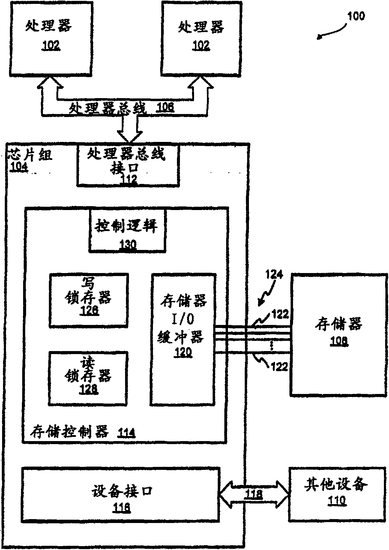
Figure 1 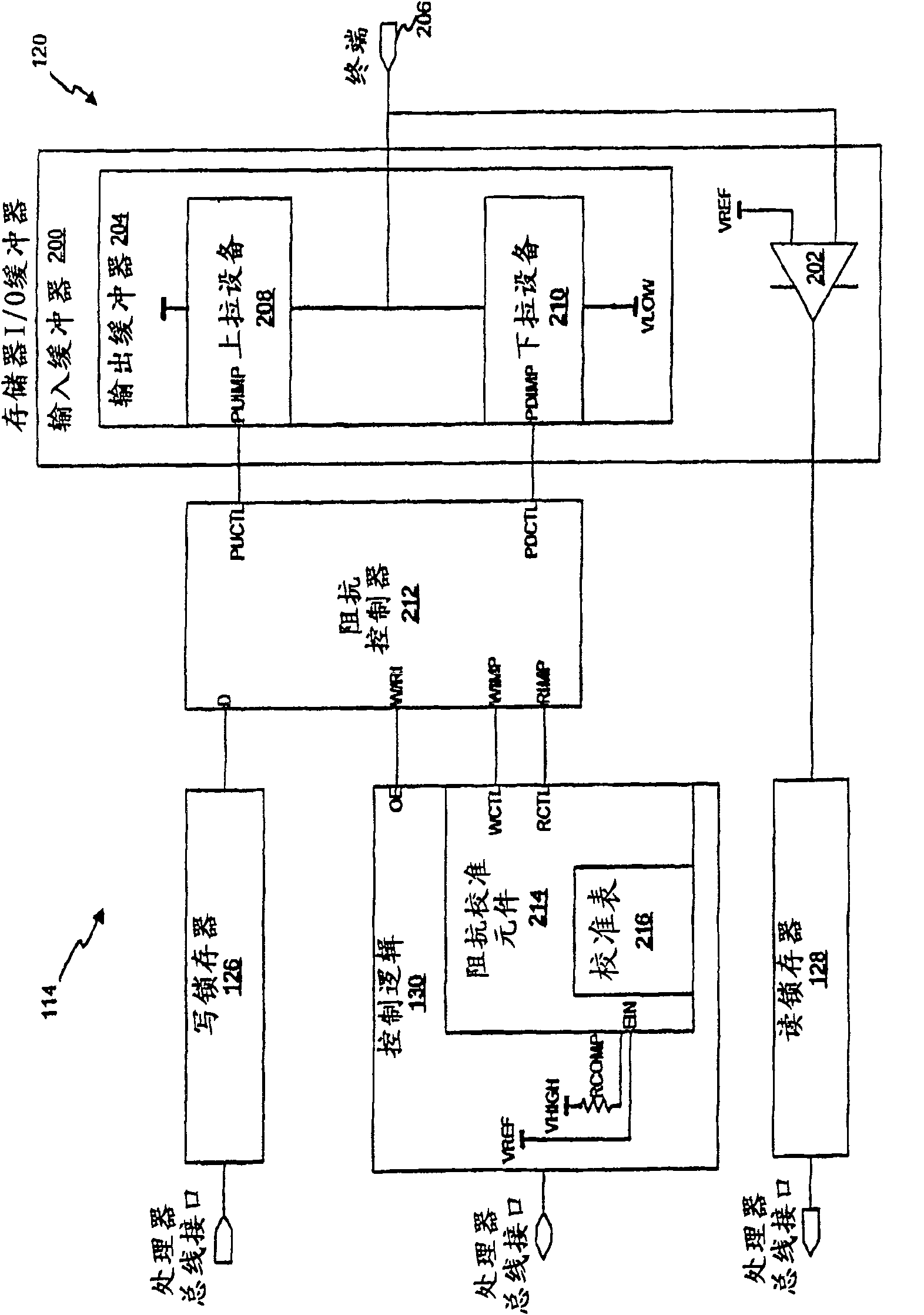
Figure 2 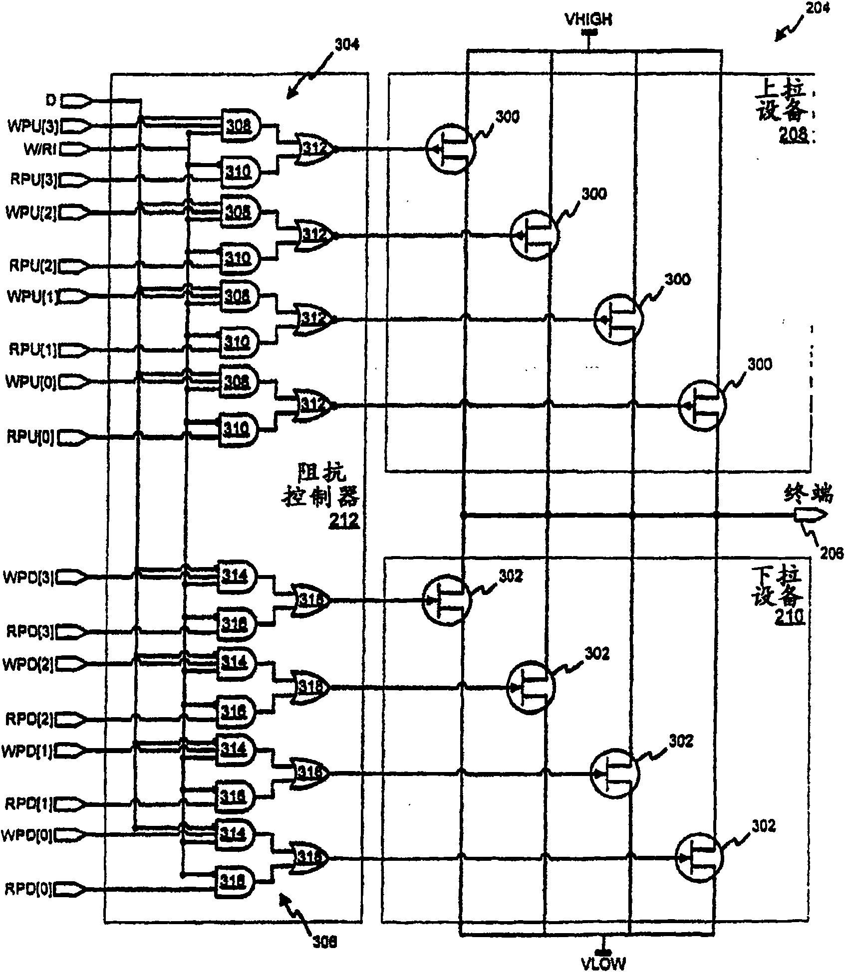
Figure 3
Abstract
Description
technical field
[0001] The present invention relates to a computing device and its memory controller and control method. Background technique
[0002] Data transfer rates between system memory and memory controllers continue to increase. To improve signal integrity at higher transfer rates, memory devices and memory controllers include termination resistors that match the impedance of the memory bus to reduce signal reflections on the memory bus. Conventional memory controllers include separate termination resistors that are connected to the memory bus during the read and / or idle states of the memory bus. Additionally, these memory controllers contain additional logic to maintain constant impedance over process, voltage, and temperature. These memory controllers further include circuitry to disconnect the termination resistors from the memory bus during memory writes. These additional termination resistors, logic, and circuitry associated with terminating the memory bus c...