Printed circuit board processing device and drilling processing method therefor

A technology for printed circuit boards and processing equipment, applied in the directions of printed circuit, printed circuit manufacturing, metal processing equipment, etc., can solve the problems of no disclosure of movement control, the overall increase of drill drilling processing equipment, and no disclosure, etc. Body vibration, reduced rocking vibration, high-precision machining effects

Inactive Publication Date: 2007-08-22
HITACHI SEIKO LTD
View PDF3 Cites 27 Cited by
  • Summary
  • Abstract
  • Description
  • Claims
  • Application Information

AI Technical Summary

Problems solved by technology

[0007] In Patent Document 1, there is no disclosure about, for example, how to improve the processing accuracy when processing printed circuit boards with the same processing content
[0008] In addition, in the case of moving the horizontal slide plate, similar to when moving the X table, vibrations in the vertical direction are generated on the bed, so if the patent document 2 The technology co

Method used


Image

  • Printed circuit board processing device and drilling processing method therefor
  • Printed circuit board processing device and drilling processing method therefor
  • Printed circuit board processing device and drilling processing method therefor

Examples


Embodiment 2

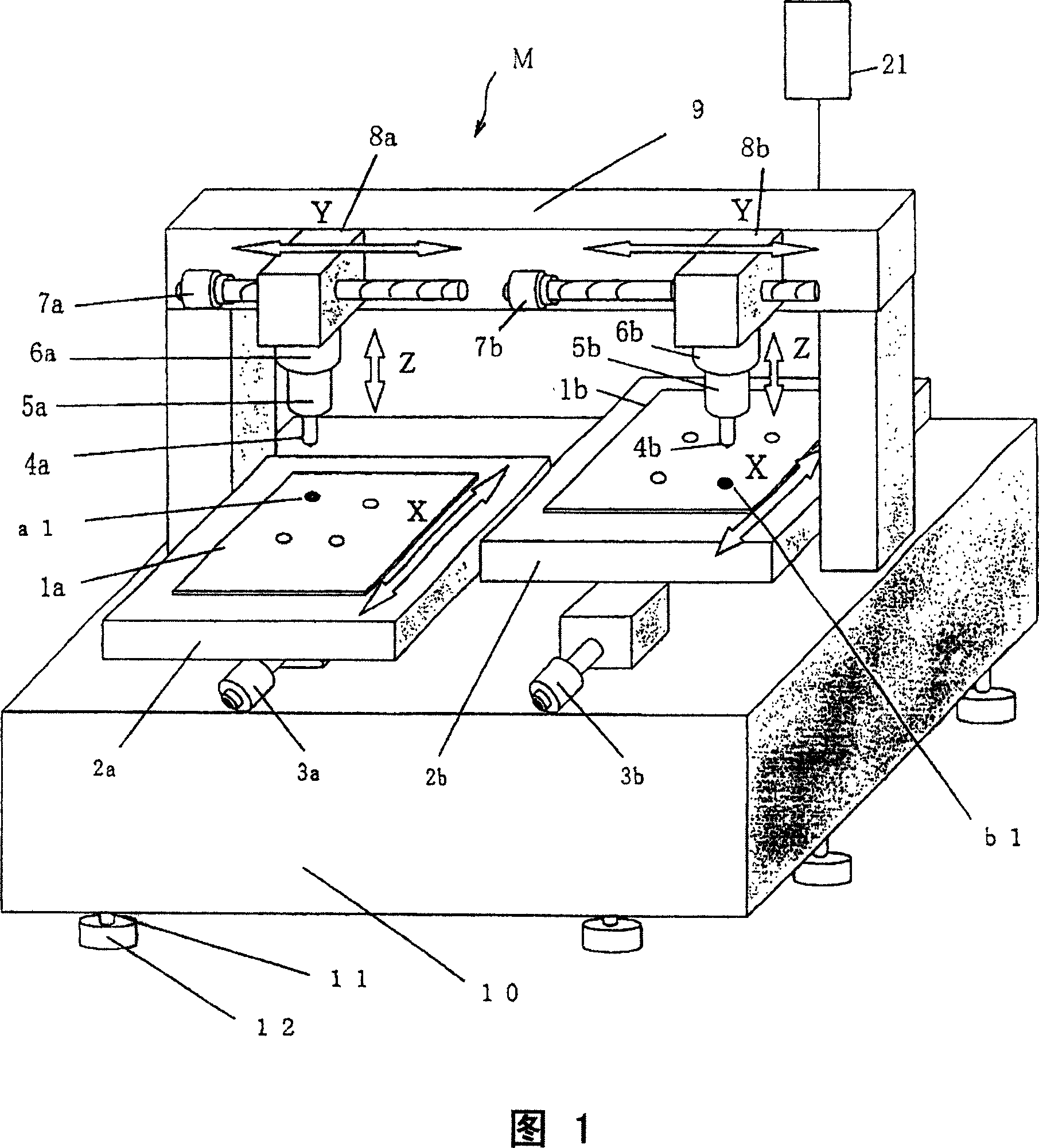
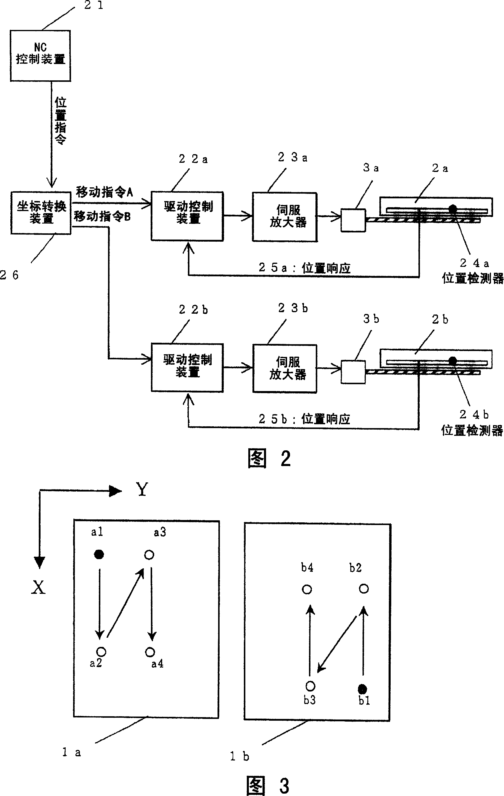
[0047] In the above-mentioned first embodiment, one of the two printed circuit boards is rotated 180° relative to the other and arranged on the table, and when the processing position is, for example, point-symmetrical or nearly point-symmetrical with respect to the center of the printed circuit board in the XY direction , as shown in FIG. 7, the directions of the printed circuit boards 1a and 1b loaded on the worktables 2a and 2b can also be set to be the same, as indicated by the arrows in the same drawing, and the processing order of the above-mentioned printed circuit boards adjacent to each other can be set to be the same. Instead, process it.

[0048] In addition, in the above-mentioned Embodiments 1 and 2, the case where the plurality of lateral sliding plates 8a, 8b are arranged on one side of the column body 9 (the front side in FIG. 1 ) was described, but it may be arranged as follows.

Embodiment 3

[0050] 8 is a plan view showing the structure of another printed circuit board processing equipment to which the present invention is applied, and the same components or components with the same functions as those in FIG. 1 are assigned the same reference numerals and description thereof will be omitted.

[0051] As shown in the same figure, this printed circuit board processing facility includes not only tables 2a, 2b and lateral slides 8a, 8b shown in FIG. 1 but also tables 2c, 2d, and lateral slides 8c, 8d.

[0052] The table 2c and the table 2a, and the table 2d and the table 2b are arranged on the bed 10 so that the moving direction of the center of gravity is coaxial. Tables 2c and 2d are freely movable in the front-back (X) direction by linear guides (not shown) and X-axis drive devices 3c and 3d. Printed circuit boards 1c, 1d are respectively arranged on workbenches 2c, 2d. In addition, the printed circuit board 1c is rotated by 180° relative to the printed circuit bo...


PUM


Abstract

The device has printed circuit boards mounted on respective tables, and a control unit controlling an X-axis drive section and a Y-axis drive section to move an X-direction axle and Y-direction axle in a direction. The axles are positioned in processing positions by the X-axis drive section and a Y-axis drive section. The axes are determined such that drills are put into a printed circuit board by a Z-axis drive section to drill holes. The z-axis drive section moves a spindle into corresponding z-direction. An independent claim is also included for a method for drilling a printed circuit board processing device.

Description

technical field [0001] The invention relates to printed circuit board processing equipment and a drilling method thereof. Background technique [0002] As printed circuit board processing equipment, there is, for example, a printed circuit board processing equipment provided with: a single bed forming a plurality of table loading areas; being integrally fixed to the above bed across the table loading areas, and A column forming a support area for a plurality of transverse slides corresponding to the loading area of ​​the workbench; at least one workbench individually movably supported on the above bed in the X direction; individually movably supported in the Y direction on the above-mentioned column at least one transverse sliding plate on the top; and individual spindle units movably supported on the transverse sliding plate along the Z direction. Since this type of printed circuit board processing equipment has a structure in which a plurality of printed circuit board pro...

Claims


Application Information

Patent Timeline
IPC IPC(8): H05K3/00
CPCH05K3/0047B23B39/161B23B39/18H05K3/0008H05K3/0097B23Q5/22H05K13/00
Inventor 渡边一雄熊谷德成长泽胜浩山下孝彦镰田弘幸腰塚久洋菅原弘之宫坂彻
Owner HITACHI SEIKO LTD
Why Eureka
Try Eureka