Physical layer chip, method for transferring the signal and switcher

A physical layer chip and physical layer technology, applied in the transmission system, electrical components, etc., to achieve the effect of reducing complexity, reducing the number, and large economic benefits

Active Publication Date: 2007-09-12
NEW H3C TECH CO LTD
View PDF0 Cites 15 Cited by
  • Summary
  • Abstract
  • Description
  • Claims
  • Application Information

AI Technical Summary

Problems solved by technology

[0006] In view of this, an object of the present invention is to provide a physical layer chip, another object of the present invention is to provide two methods for transmitting signals at the Ethernet physical layer, and another object of the present invention is to provide a switch such that a An optical port module with a higher rate can replace two or more optical port modules with a lower rate, thereby reducing the cost of the physical layer chip and the complexity of networking, or solving the complexity and complexity of networking at an acceptable cost. Qos problem

Method used


Image

  • Physical layer chip, method for transferring the signal and switcher
  • Physical layer chip, method for transferring the signal and switcher
  • Physical layer chip, method for transferring the signal and switcher

Examples


Embodiment Construction

[0047] The present invention will be further described in detail below in conjunction with the accompanying drawings and specific embodiments.

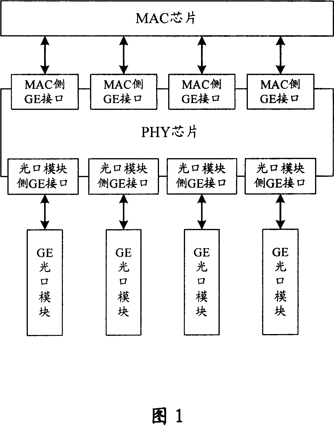
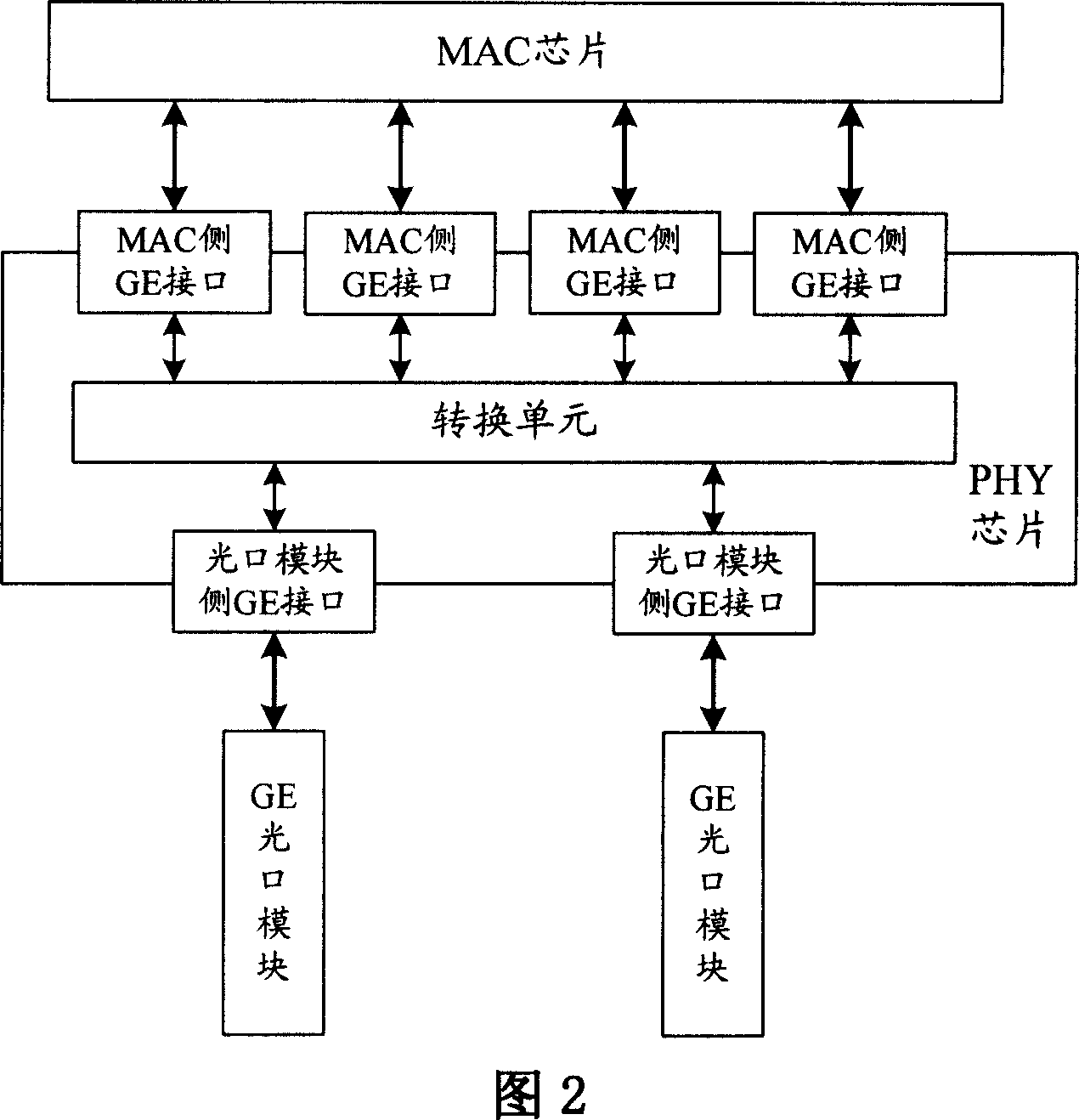
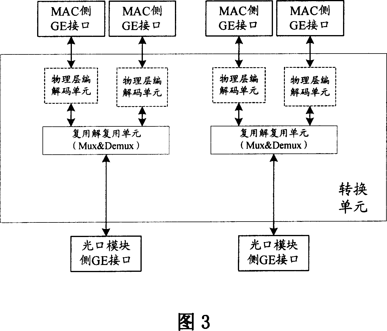
[0048] FIG. 2 is a schematic diagram of signal transmission through the inventive PHY chip, and at the same time, this figure also shows a schematic structural diagram of the PHY chip of the present invention. Referring to FIG. 2 , the PHY chip of the present invention is also used to transmit signals between the MAC chip and the optical port module. In addition to the low-speed GE interface on the MAC side and the high-speed GE interface on the optical port module side, the PHY chip also includes a conversion unit. The conversion unit is used to receive M low-speed signals from the MAC layer through the low-speed GE interface on the MAC side, multiplex the M signals into N high-speed signals, determine the optical port module corresponding to the N signals, and pass through the optical port The high-speed GE interface on the module ...


PUM


Abstract

This invention discloses a physical layer chip, used between the MAC chip and the mouth modules to transmit signal, the physical layer chips including conversion modules for low-speed side signals multiplexing M from the MAC duplicate N road for high-speed optical signal transmitted to the mouth module or for the modules from the light side of the mouth high-speed interface N road signals for M Road after low-speed signals transmitted to the MAC chip. The present invention also discloses two Ethernet physical layer signal transmission method for the MAC chip and optical modules mouth between the signal multiplexing and discloses an application of this technology to the switch. This invention makes a greater rate-mouth module can replace two or more smaller rate optical module mouth, decreasing the physical layer interface chip number and reducing the physical layer chip itself costs, and further reducing the cost of the equipment, and the realization of the complexity, which can be accessed and resolved within the cost of network complexity and Qos issues.

Description

technical field [0001] The invention relates to the technical field of physical layer chips, in particular to a physical layer chip, a signal transmission method and a switch. Background technique [0002] The specifications of Ethernet media access control (MAC) chips and physical layer (PHY) chips currently on the market include 10 / 100M adaptive, 1GE (that is, a GE interface with a transmission rate of 1G bits), and 2.5GE (that is, a transmission rate of 2.5G bit GE interface) and 10GE (that is, a GE interface with a transmission rate of 10G bit), etc. Generally, according to the type of external GE interface, PHY chips can be roughly divided into optical port PHY chips, electrical port PHY chips, and wireless port PHY chips. From the current actual application situation, the main function of the optical port PHY chip is to complete the coding of the physical layer, such as 8b / 10b conversion, filling, demarcation and other functions. Of course, all or part of these functi...

Claims


Application Information

Patent Timeline
Patent Type & Authority Applications(China)
IPC IPC(8): H04L29/10
Inventor 于洋
Owner NEW H3C TECH CO LTD
Why Eureka
Try Eureka