Printed circuit board printing system and method

A technology of printed circuit boards and printed systems, applied in the directions of printed circuits, printed circuits, printed circuit manufacturing, etc., can solve problems such as accumulation and aggravation

Inactive Publication Date: 2007-09-12
HEWLETT PACKARD DEV CO LP
View PDF0 Cites 8 Cited by
  • Summary
  • Abstract
  • Description
  • Claims
  • Application Information

AI Technical Summary

Problems solved by technology

As a result, the time, cost, materials and other factors of the photolithograph

Method used


Image

  • Printed circuit board printing system and method
  • Printed circuit board printing system and method
  • Printed circuit board printing system and method

Examples


Embodiment Construction

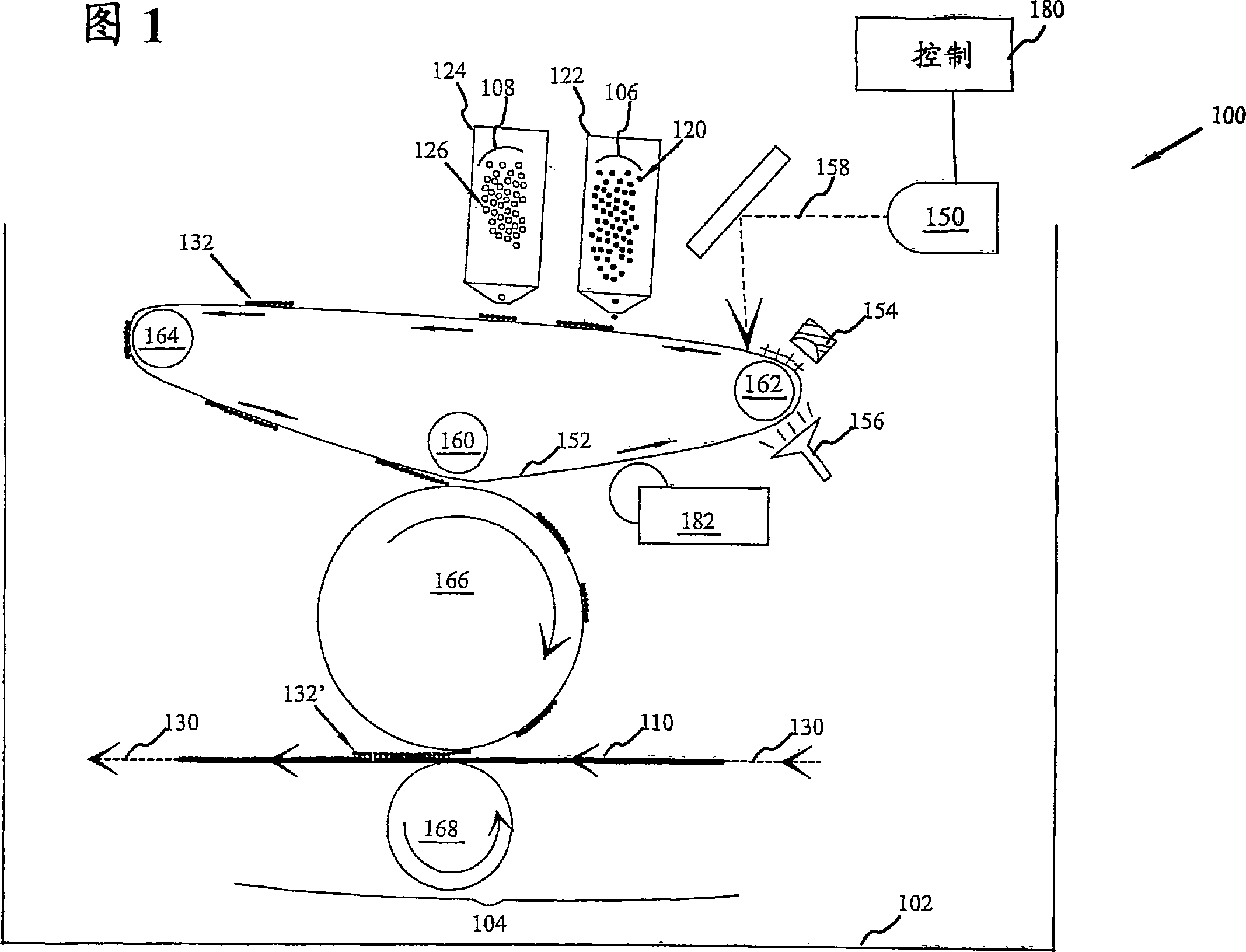
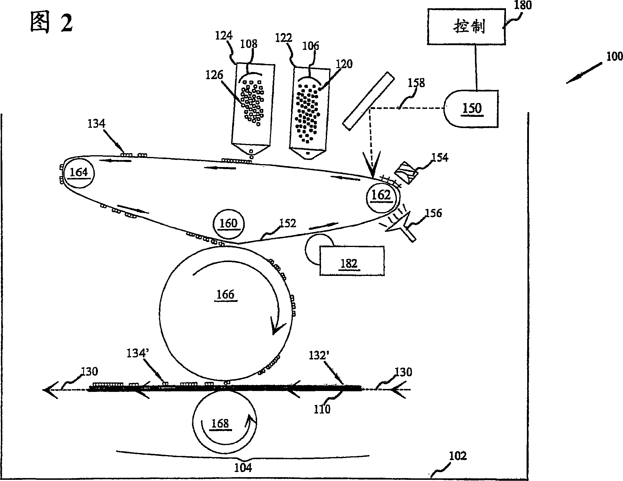
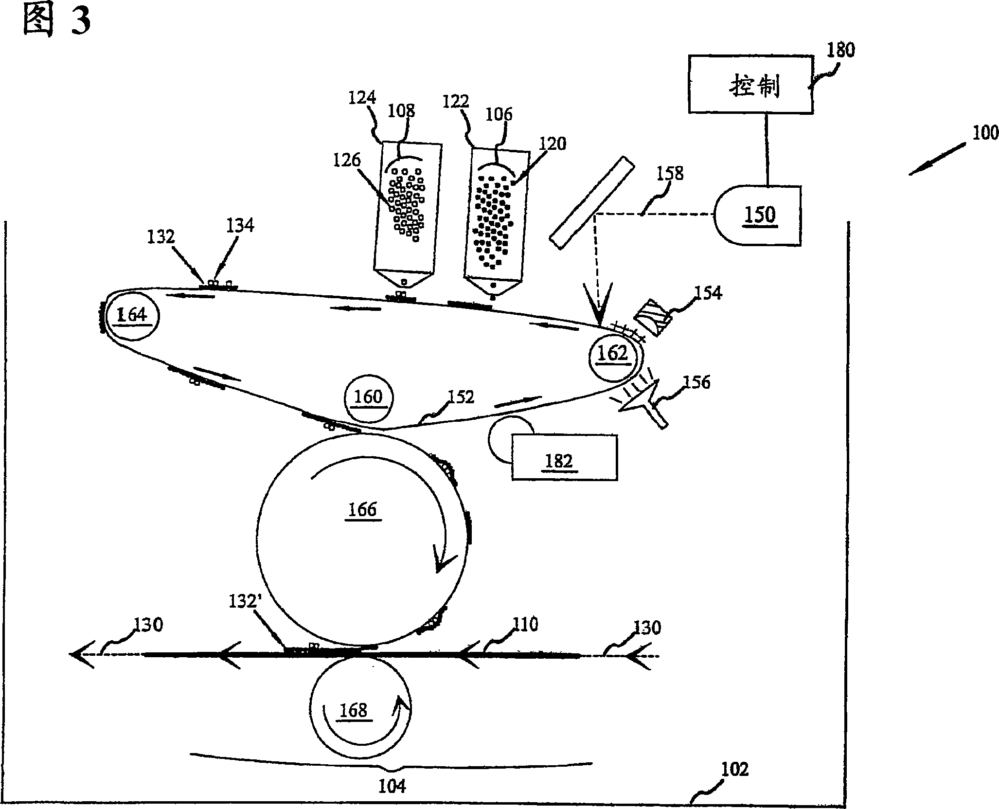
[0032] Before beginning to describe specific embodiments, it is to be realized that the description of the invention has been made by way of example and not limitation. The concepts herein are not limited to use or application to a particular type of printed circuit board (PCB) printing system. Thus, while the tools described herein are provided for ease of explanation and have been illustrated and described with reference to exemplary embodiments, it will be appreciated that the principles herein may be equally applied to other types of printed circuit board (PCB) printing system. It will be appreciated that the drawings are not necessarily to scale and may have been exaggerated in some respects for ease of discussion.

[0033] Referring now to the drawings, and more particularly to FIG. 1 , there is shown a portion of a PCB printing system 100 having a housing 120 , at least one liquid electrophotographic printing device 104 , at least one conductive ink provider 106 , in a...


PUM


Abstract

The invention provides a printed circuit board (PCB) printing system. In a particular embodiment, the system includes a liquid electrophotographic printing device. At least one supplier of electrically conductive ink supplying electrically conductive ink to the electrophotographic printing device is also provided. In addition, at least one supplier of dielectric ink supplying dielectric ink to the electrophotographic printing device is also provided. The liquid electrophotographic printing device is operable to apply the electrically conductive ink and the dielectric ink to a provided substrate such that substantially immiscible boundary delineation occurs at any points of contact between the applied electrically conducive ink and the applied dielectric ink. An appropriate method of use for the rendering of a printed circuit board is also provided.

Description

technical field [0001] The present invention relates generally to systems and methods for printing printed circuit boards, and more particularly to the use of liquid electrophotographic printing in printing printed circuit boards. Background technique [0002] Computers, televisions, communication equipment, consumer electronics, and most electronic devices rely on printed circuit boards (PCBs) to interconnect and interface the electronic components inside. For example, the PCB, known as a computer motherboard, provides the interconnections and interfaces between memory, processors, switches, and many other components that collectively operate as a desktop or laptop computer. In other words, a PCB is a platform where other electronic devices are connected together to interact as larger systems and devices. [0003] Early PCBs were relatively simple because of the low component count and the size and complexity of the connected components. As electronic components and devic...

Claims


Application Information

Patent Timeline
IPC IPC(8): H05K3/12H05K3/20
CPCY02B60/33H05K3/207H04L45/245H05K2201/0257H05K2203/0517H05K3/1266H04L45/00H04L45/60H04L45/24H05K2203/0126G03G15/10G03G15/224G03G15/6585Y02D30/50
Inventor M·夏马L·T·特兰
Owner HEWLETT PACKARD DEV CO LP
Why Eureka
Try Eureka