Multiple clock system integrative circuit plane layout method
An integrated circuit and plane layout technology, applied in the direction of electrical digital data processing, special data processing applications, instruments, etc., can solve the problem of not considering the connection relationship of the clock area
- Summary
- Abstract
- Description
- Claims
- Application Information
AI Technical Summary
Problems solved by technology
Method used
Image
Examples
Embodiment Construction
[0041] The method of the present invention is further described below through two standard test examples.
[0042] (1) Read layout standard test cases, store the area, length and width, type, connection and clock information of each module;
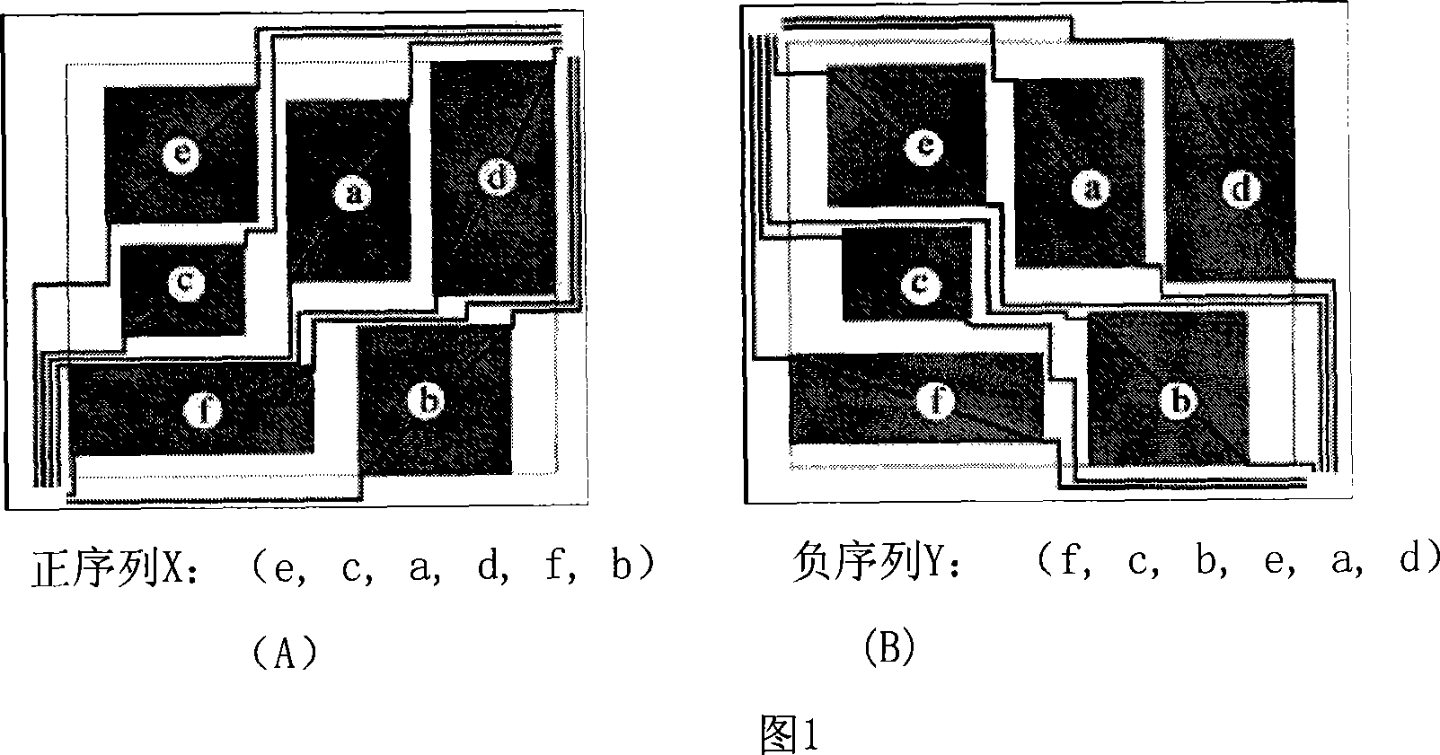
[0043] (2) Select the initial sequence pair: Since the simulated annealing optimization has nothing to do with the initial solution, the serial numbers of the modules can be taken in clock order to form a sequence pair, which can satisfy the constraint condition (1). At the same time, in the following simulated annealing process, the operation of the sequence pair Keep the serial numbers corresponding to the same clock module always adjacent;
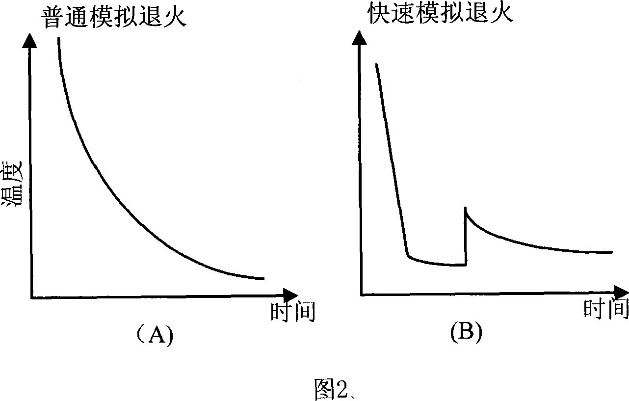
[0044] (3) First, the simulated annealing method is used to optimize to find the optimal solution of the objective function. This process is mainly optimized for the constraints of the connection relationship between different clock regions: set the initial annealing temperature to 1, and the termi...
PUM
 Abstract
Description
Claims
Application Information


