Packaging method for white light illuminating diode

A technology for light-emitting diodes and packaging methods, applied in electrical components, circuits, semiconductor devices, etc., can solve the problems of reducing white light-emitting diodes, the lifespan of white light-emitting diodes is not long enough, and limiting the application of white light-emitting diodes, etc. The effect of decay

Inactive Publication Date: 2007-11-07
NINGBO ANDY OPTOELECTRONIC CO LTD
0 Cites 27 Cited by

AI-Extracted Technical Summary

Problems solved by technology

[0004] However, at present, the above-mentioned various measures basically do not significantly reduce the light decay of white light emitting diodes, and the actual life of white light emitting diodes is still not long enough, which largely limits the application of white lig...

Method used

The present invention is produced on the basis of a large number of experiments, and the contriver is through a series of experiments, carries out matching test with the chip of a large amount of packaging materials and light-emitting diodes, finally finds that use is made of polydimethylsilicon...

Abstract

This invention relates to a packaging method for white light LED including the following steps: dropping insulation glue in a reflection ring of a frame, placing prepared grains on a frame dropped with insulation glue, baking the fixed semiconductor grains to adhere them fixedly, leading two wires from the baked grains at the positive and negative, configuring fluorescent powder and taking out polydimethyl silicon ketone, fixing agent for packaging LED and fluorescent powder to be mixed fully, dropping the prepared mixed fluorescent powder in the frame reflection ring welded with wires then to be baked and solidified, preparing glue, filling the glue and baking it.

Application Domain

Technology Topic

Image

  • Packaging method for white light illuminating diode
  • Packaging method for white light illuminating diode
  • Packaging method for white light illuminating diode

Examples

  • Experimental program(1)

Example Embodiment

[0029] The white light-emitting diode packaged according to the packaging method of the present invention includes a bracket, a light-emitting diode die, a powder-dispensing glue and a phosphor. The light-emitting diode die is fixed on the bracket, and the phosphor and the powder-dispensing glue are mixed in proportion. The powder-mixing glue is formed by proportioning polydimethyl silicone and curing agent for LED encapsulation.
[0030] Please refer to FIG. 5, the packaging process of the white light emitting diode disclosed in this embodiment includes the following steps:
[0031] Step 1: Dispensing glue, that is, dispensing insulating glue into the reflector cup of the bracket.
[0032] Step 2: Bonding, that is, placing the prepared die on the support of the insulating glue.
[0033] Step 3: Baking after solidification, that is, putting the semi-finished product with solid crystal grains into a high-temperature oven for baking, so that the crystal grains are fixed and adhered to the bracket.
[0034] Step 4: Wire bonding, that is, two gold wires are drawn from the baked crystal grains on the positive and negative electrodes.
[0035] Step 5: Preparing phosphors, that is, take out polydimethyl silicone, curing agent for LED encapsulation, and carbonate phosphors in a ratio of 3:3:1 (quality, the same below) for preparation, and then stir to make It is thoroughly mixed, and the stirring time is about 5 minutes.
[0036] Step 6: Vacuuming, that is, vacuum degassing the formulation made of polydimethyl silicone, curing agent for LED encapsulation, and carbonate phosphor. The vacuuming time is about 5-10 minutes.
[0037] Step 7: Point the phosphor, which is about to be vacuumed and pour the mixture made of polydimethyl silicone, curing agent for LED encapsulation, and phosphor powder into the syringe of the dispenser. After adjusting the amount of glue , And point them into the reflector cup of the bracket where the gold wire has been welded.
[0038] Step 8: Bake after lighting the phosphor. Put the bracket with the phosphor into a high-temperature oven for curing, at a temperature of 130-150 degrees, and a baking time of 1-2 hours.
[0039] Step 9: Dispense glue, that is, prepare the pre-heated epoxy glue of agent A and B according to a certain ratio, generally 1:1, and stir it so that it is fully mixed.
[0040] Step 10: Vacuum, that is, vacuum degas the formulation prepared in Step 9, and the vacuum time is about 5-10 minutes.
[0041] Step 11: Pouring glue, that is, using a glue pouring machine to sequentially inject glue into the mold cavity or bracket.
[0042] Step 12: Bake after pouring the glue, that is, high-temperature baking is performed to solidify the glue injected in Step 11, the baking temperature is 125 degrees, and the time is 8-10 hours.
[0043] Step 13: Cut the feet: Use a stamping die to separate the positive and negative poles.
[0044] Step 14: Spectroscopy, that is, use a spectrometer to classify the products according to the relevant electrical parameters such as voltage, brightness, and color.
[0045] In this embodiment, the chip uses a light-emitting diode die with a blue light emission wavelength of 455-465nm, an insulating glue for the bonding glue (of course, silver paste can also be used), and a silicate fluorescent powder (of course also It is YAG yttrium aluminum garnet phosphor, TAG terbium aluminum garnet phosphor or sulfide phosphor, etc.), the light emitting diode bracket adopts iron bracket (of course, copper bracket can also be used), and the powder glue is made of polydimethyl Curing agent for silicone and light-emitting diode encapsulation (dibutyltin dilaurate is used in this embodiment, of course, it can also be acid and alkali or lead, cobalt, tin, iron and others that can act as a catalyst for the silanol condensation reaction Soluble organic salts of metals) are formed in proportions. In this embodiment, the ratio of polydimethyl silicone and curing agent for light-emitting diode encapsulation is 1:1, and the viscosity of the powdered adhesive is 3.8pa. s, the viscosity of the polydimethyl silicone before blending is 5.7 pa.s, the viscosity of the curing agent before blending is 3.2 pa.s, the phosphor, polydimethyl silicone, and light-emitting diode encapsulation The mixing ratio (mass) of the curing agent is 1:3:3.
[0046] In order to verify the light decay condition of the white light emitting diode packaged by the above packaging method, the present invention has done a lot of experiments. Please refer to Figure 6, which shows the same situation, when using standard 20mA current drive, using polydimethyl silicone and light-emitting diode packaging curing agent formulations for packaging, silicone packaging and epoxy resin packaging Curve graph of the results of the light decay experiment. From the figure, we can see that the serial number 1 is a traditional silicone encapsulated product. At 168 hours, there is only 1% light attenuation, but at 336 hours, there is a 7% attenuation, and at 1000 hours, its light attenuation rate Reached 28%. No. 2 is a product encapsulated by epoxy resin. It has a light decay rate of 8% at 168 hours, 16% at 336 hours, and 54% at 1000 hours, which is very serious. No. 3 is the product disclosed in the present invention that uses polydimethyl silicone and a curing agent formulation for light-emitting diode encapsulation for encapsulation. At 168 hours, its luminous flux has increased by 4%, and at 336 hours, it has maintained a 4% increase. At 1000 hours, there is still no light attenuation, and it still keeps increasing by 3%.
[0047] In order to further verify the light decay condition of the white light emitting diode encapsulated by polydimethyl silicone and the curing agent formulation for light emitting diode encapsulation disclosed in the present invention, the inventors used the standard 40mA current to drive the light decay condition. A lot of experiments. Please refer to Figure 7, which shows the use of polydimethyl silicone and light-emitting diode encapsulation curing agent formulations disclosed by the present invention for encapsulation and traditional silicone encapsulation and epoxy resin when driving with a standard 40mA current A graph of the results of the light decay experiment on the package. From the figure, we can see that the serial number 1 is a traditional silicone encapsulated product, which has a light decay rate of 42% at 168 hours, and a light decay rate of 65% at 504 hours. The light attenuation is very serious. The serial number 2 is an epoxy resin encapsulated product. The light decay rate is 41% at 168 hours, and the light decay rate reaches 79% at 500 hours, and the light attenuation is very serious. No. 3 is the product disclosed in the present invention that uses polydimethyl silicone and a curing agent formulation for light-emitting diode encapsulation for encapsulation. At 168 hours, its luminous flux increased by 3%, and at 504 hours, it still maintained a 3% increase. Rate, there is still no light attenuation. It can be seen that the white light emitting diode encapsulated by the encapsulation method disclosed in the present invention has a very low light decay and a longer life span than products encapsulated by epoxy resin or traditional silicone on the market.
[0048] It should be noted that the same situation mentioned above means: (1) Each experiment is carried out in the same laboratory, under the same time period and environmental conditions; (2) Each test item is randomly selected from a number of single tubes Among them, 20 light-emitting diodes were used as test samples.
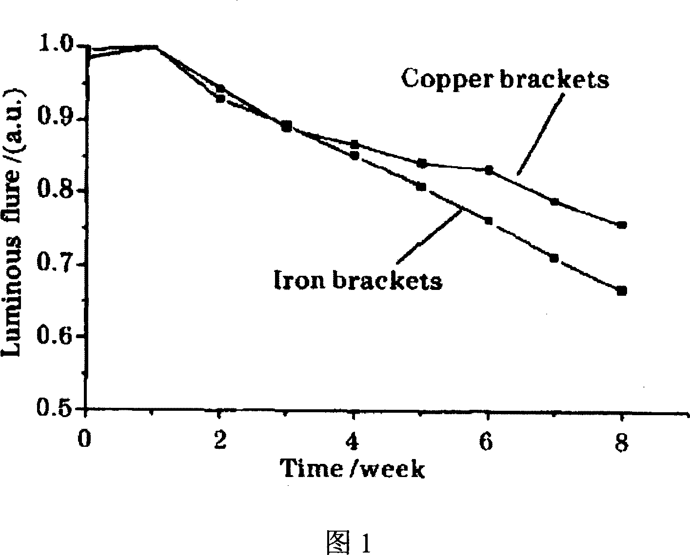
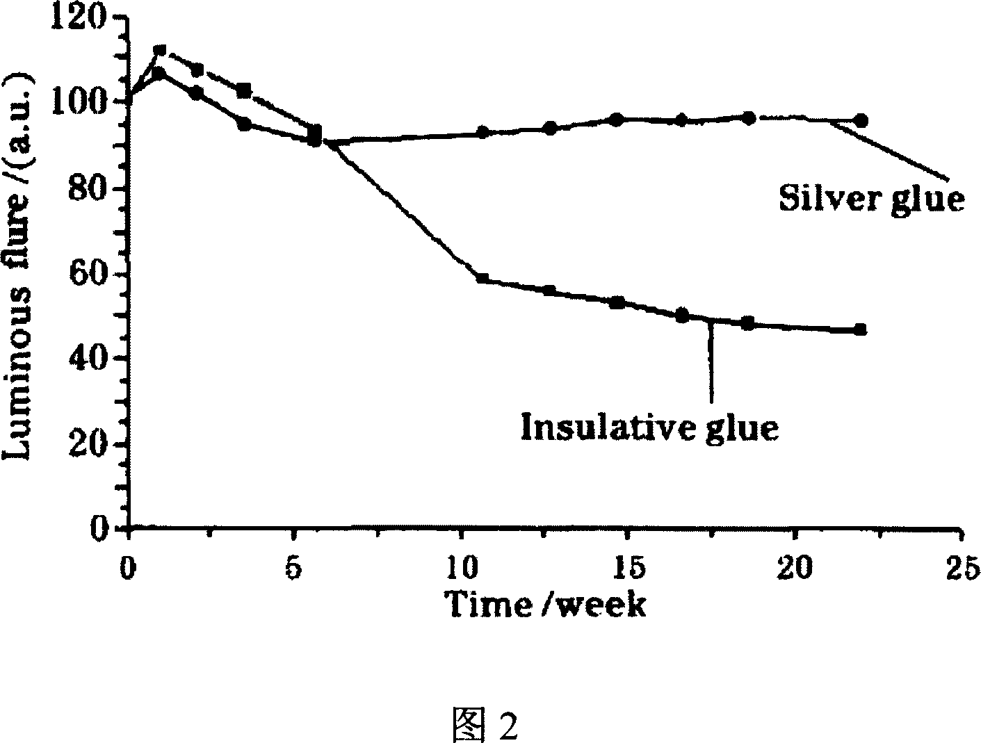
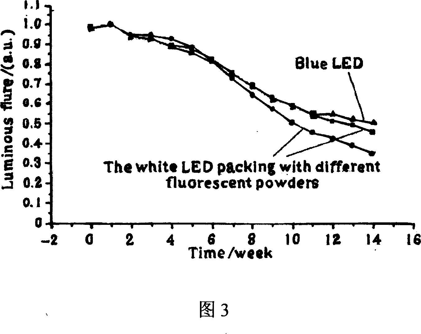
[0049] The present invention is produced on the basis of a large number of experiments. After a series of experiments, the inventor tested a large number of packaging materials and light-emitting diode chips, and finally found that the use of polydimethyl silicone and light-emitting diode packaging curing The formulation of the agent in proportion to powder encapsulation can greatly reduce the light decay rate of the white light emitting diode and significantly increase the life of the white light emitting diode.
[0050] The above description is only the embodiments of the present invention. It should be understood that without departing from the concept of the present invention, simple modifications and replacements of the present invention should be included in the technical concept of the present invention.

PUM

no PUM

Description & Claims & Application Information

We can also present the details of the Description, Claims and Application information to help users get a comprehensive understanding of the technical details of the patent, such as background art, summary of invention, brief description of drawings, description of embodiments, and other original content. On the other hand, users can also determine the specific scope of protection of the technology through the list of claims; as well as understand the changes in the life cycle of the technology with the presentation of the patent timeline. Login to view more.

Similar technology patents

Light-emitting diode packaging method

InactiveCN101071834AReduce light decay rateSemiconductor devicesCrystalliteWork in process
Owner:NINGBO ANDY OPTOELECTRONIC CO LTD

Method, system and device for controlling vehicle power device and storage medium

ActiveCN108394401AAvoid violent dynamic load changesExtend your lifeTransportation hydrogen technologyAutomotive engineeringEngineering
Owner:TSINGHUA UNIV

Metal drawing oil

InactiveCN103031189AReduce heatExtend your lifeAdditivesViscosity indexAntioxidant
Owner:LOCKS LUBE SHANGHAI

Classification and recommendation of technical efficacy words

Why Eureka
Try Eureka