

PI solution method based on IC package PCB co-design
A collaborative design and solution technology, applied in computing, instrumentation, electrical and digital data processing, etc., can solve the problems of noise, large and serious package parasitic inductance, etc.
Active Publication Date: 2007-11-14
INST OF MICROELECTRONICS CHINESE ACAD OF SCI
View PDF0 Cites 18 Cited by
- Summary
- Abstract
- Description
- Claims
- Application Information
AI Technical Summary
Problems solved by technology
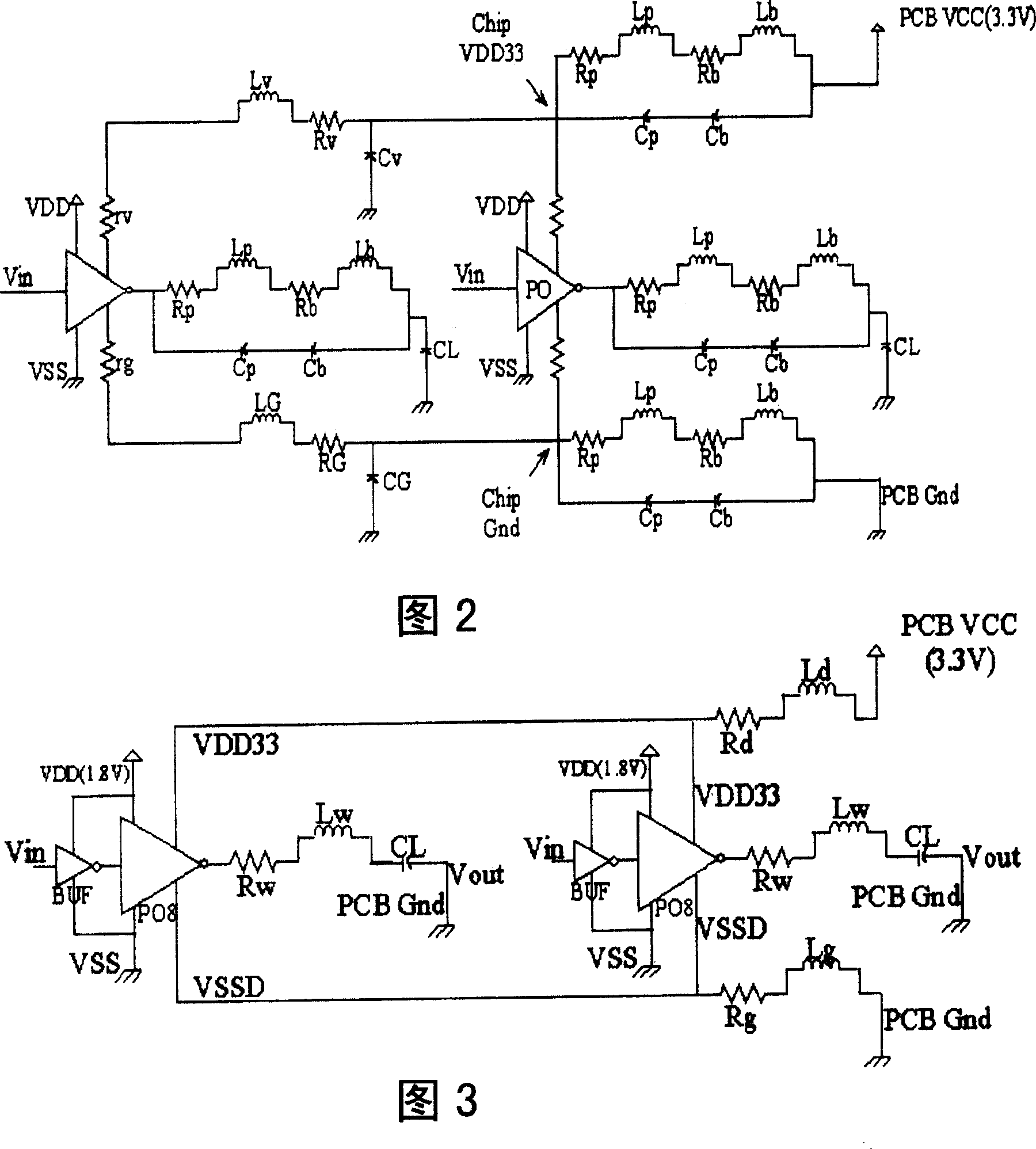
[0007] The output unit is the main noise source of synchronous switching noise, because the large switching current flowing through its ground wire and package parasitic inductance changes very rapidly, and the package parasitic inductance is also relatively large, so the noise generated is serious
As the scale of integrated circuits becomes larger, it is difficult for designers to model and simulate simultaneous switching noise for the entire design
Method used
View moreImage
Smart ImageViewing Examples

Examples
specific Embodiment
[0066] The invention has been applied in the IC-packaging-PCB collaborative design process of the KW0501 4.5 million-gate DSP of the Institute of Microelectronics, which adopts the SMIC 0.18um CMOS technology. The results of the chip test show the effectiveness and practicality of the PI solution.
Login to View More PUM
 Abstract
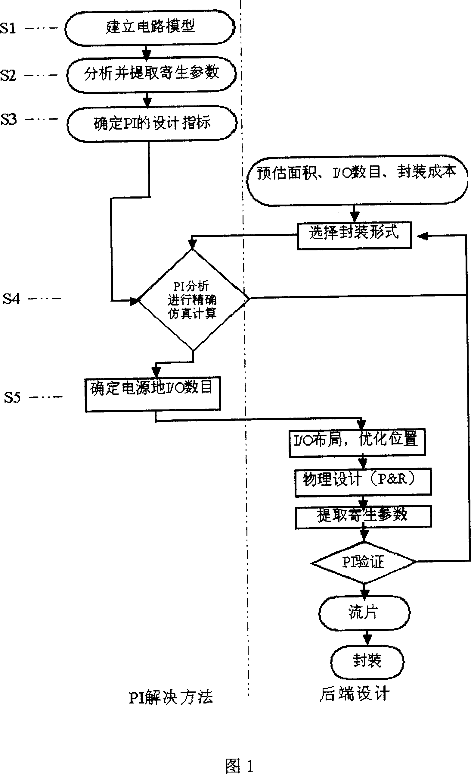
The invention relates to the field of very large scale integrated (VLSI) circuit technique, especially a PI solving method for IC-package-PCB cooperative design for solving power supply integrity problem in back-end design, comprising: 1) building a circuit model suitable for VLSI PI analysis; 2) analyzing and extracting parasitical parameters corresponding to the circuit mode; 3) determining design indexes in the PI design; 4) utilizing EDA tool and owned algorithm model to make accurate simulation and calculation; 5) on the premise of considering power supply integrity, according to the PI design indexes and simulated results, quickly determining a proper number of I / Os of power supply.
Description
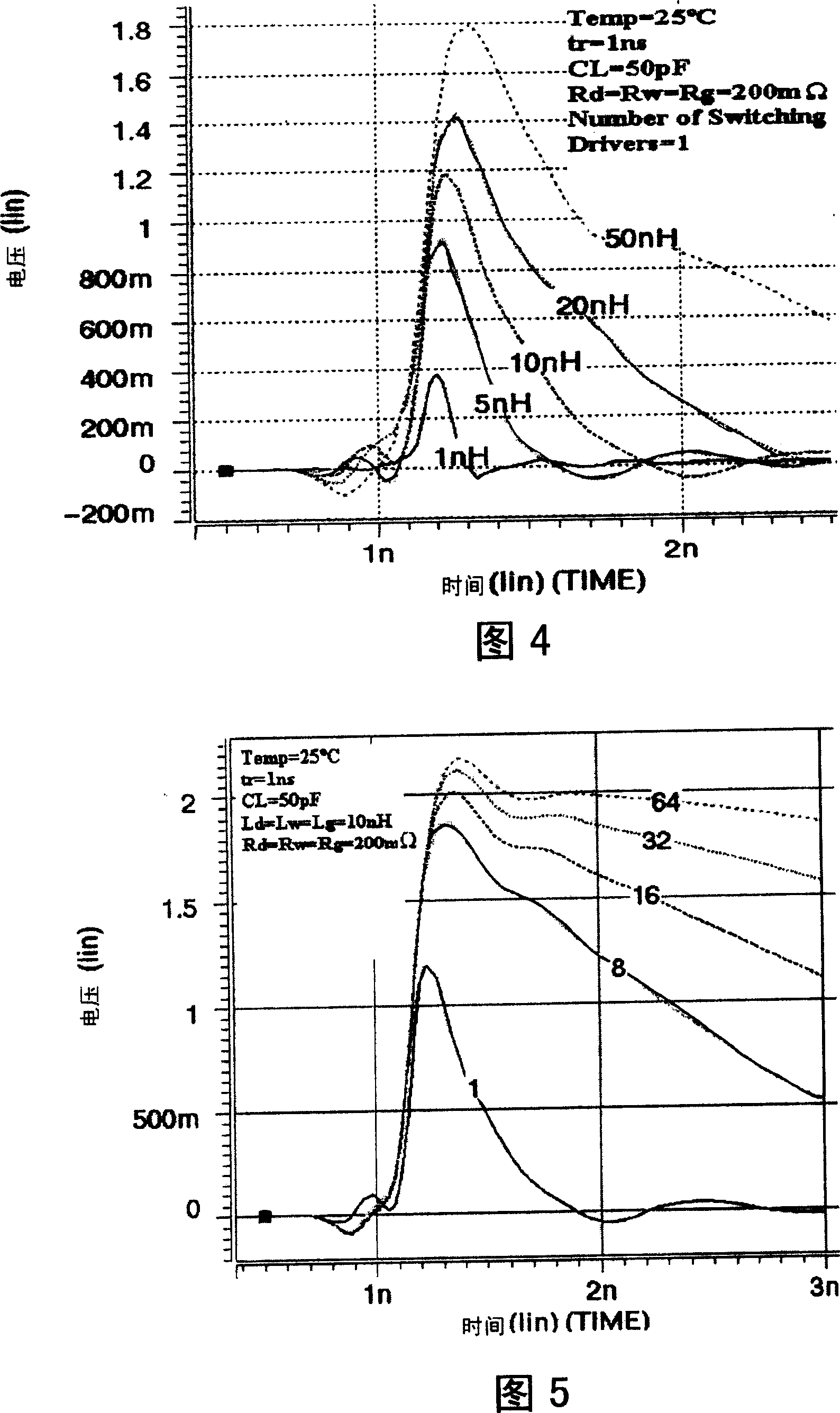
technical field [0001] The invention relates to the technical field of very large-scale integrated circuits (VLSI), in particular to a PI solution method of IC-packaging-PCB collaborative design for solving power integrity problems in back-end design. Background technique [0002] As the working speed and integration of integrated circuits (ICs) are getting higher and higher, the chip functions are getting more and more, the chip power consumption is getting bigger and bigger, and the flipping frequency of the unit is getting higher and higher, which also brings chip input and output increase in pins. These may cause noise on the power supply and ground, resulting in a decrease in the performance of the integrated circuit chip, or even malfunction of the function, which brings about the problem of power integrity, which will affect the convergence of the timing, the success of the design, and the power consumption. The size and stability of the chip work. While the process...
Claims
Login to View More Application Information
Patent Timeline
 IPC IPC(8): G06F17/50
Inventor刘海南周玉梅吴斌蒋见花霍津哲
OwnerINST OF MICROELECTRONICS CHINESE ACAD OF SCI