Method for manufacturing transistor structure

一种晶体管、半导体的技术,应用在晶体管、半导体/固态器件制造、半导体器件等方向,能够解决解决方案困扰技术人员、没有给出或暗示解决方案等问题

Active Publication Date: 2007-11-21
INT BUSINESS MASCH CORP +1
View PDF1 Cites 15 Cited by
  • Summary
  • Abstract
  • Description
  • Claims
  • Application Information

AI Technical Summary

Problems solved by technology

[0022] Solutions to these problems have been long sought, but existing developments have not given or suggested any solutions, and thus solutions to these problems have long eluded those skilled in the art.

Method used


Image

  • Method for manufacturing transistor structure
  • Method for manufacturing transistor structure
  • Method for manufacturing transistor structure

Examples


no. 1 example

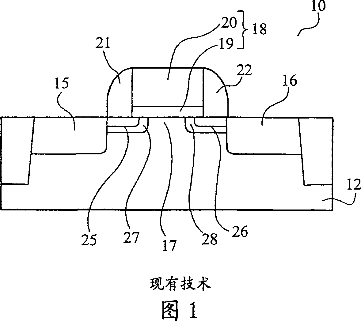
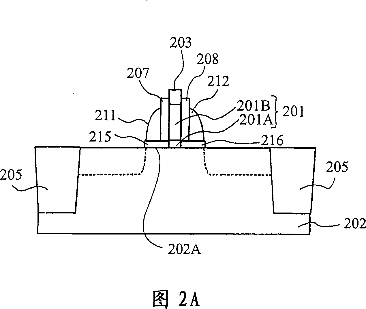
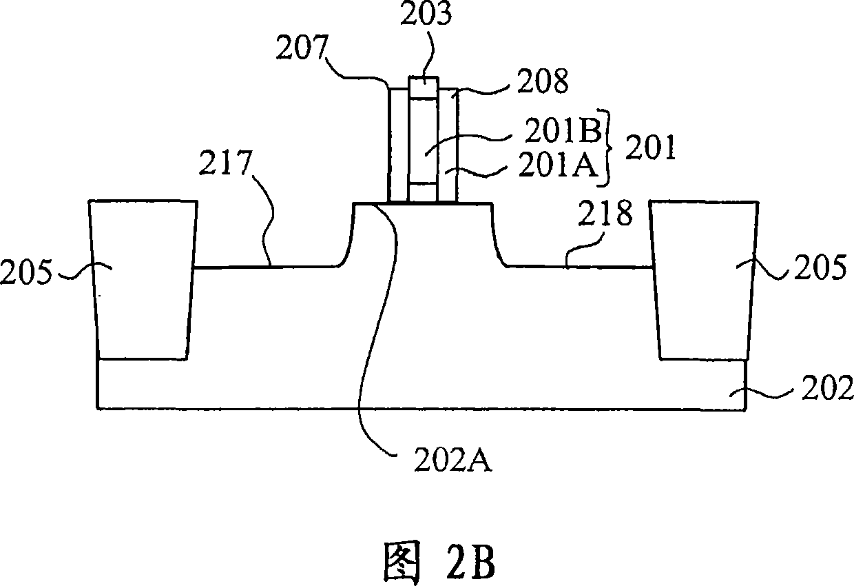
[0045] According to the first embodiment of the invention, the disposable oxide spacer elements 215, 216 are consumed during the formation of the first portion 217, 218 of the deep stress body recess. Advantageously, fabrication process parameters such as the thickness of the disposable oxide spacer elements 215, 216, etch conditions, and other parameters are adjusted such that approximately at the same time as the formation of the stressor recessed first portions 217, 218 is completed, the The exposed portions of the disposable oxide spacer elements 215, 216 are fully consumed. Advantageously, an etch with low selectivity between the substrate material and the disposable oxide isolation elements 215, 216 is used.

[0046] Advantageously, reactive ion etching of source and drain stressor recessing is performed using a gaseous etchant comprising a flowing gas mixture. The mixture of flowing gases may include: HBr, O2, He, Cl2, SF6, N2 (alone or in combination) at a flow rate f...


PUM


Abstract

The present invention relates to semiconductor integrated circuits. More particularly, but not exclusively, the invention relates to strained channel complimentary metal oxide semiconductor (CMOS) transistor structures and fabrication methods thereof. There is provided a method of forming a strained channel transistor structure on a substrate, comprising the steps of: forming a source stressor recess comprising a deep source recess and a source extension recess; forming a drain stressor recess comprising a deep drain recess and a drain extension recess; and subsequently forming a source stressor in said source stressor recess and a drain stressor in said drain stressor recess. The deep source / drain and source / drain extension stressors are formed by an uninterrupted etch process and an uninterrupted epitaxy process.

Description

technical field [0001] The present invention relates to semiconductor integrated circuits. More particularly, but not exclusively, the present invention relates to strained-channel complementary metal-oxide-semiconductor (CMOS) transistor structures and methods of fabrication thereof. Background technique [0002] Integrated circuits containing thousands of semiconductor devices play an important role in many fields of technology. The continued development of devices with high performance at reasonable cost is important to the future development of some of these technologies. Metal Oxide Semiconductor Field Effect Transistors (MOSFETs) are commonly used in semiconductor integrated circuits. It has been demonstrated that the performance of MOSFET devices can be enhanced by applying mechanical stress to parts of the device. [0003] A known MOSFET 10 is schematically shown in Figure 1 (Prior Art). MOSFET 10 is typically fabricated on a semiconductor substrate 12, such as s...

Claims


Application Information

Patent Timeline
Patent Type & Authority Applications(China)
IPC IPC(8): H01L21/336H01L21/8238
CPCH01L29/165H01L29/66636H01L29/7848H01L29/66628H01L21/3065H01L29/6659H01L29/6653H01L21/31116
Inventor 张永富K·K·德茨富利安骆志炯朱慧珑
Owner INT BUSINESS MASCH CORP
Why Eureka
Try Eureka