
Strained channel transistor and method of fabrication thereof

a technology of straining channel transistor and fabrication method, which is applied in the direction of basic electric elements, semiconductor devices, electrical equipment, etc., can solve the problems of difficult control, difficult to achieve in practice, and breakdown conditions, so as to improve short channel behaviour, improve the stress along the channel, and improve the strain in the channel.

Inactive Publication Date: 2010-08-10
TAIWAN SEMICON MFG CO LTD +1
View PDF3 Cites 4 Cited by
  • Summary
  • Abstract
  • Description
  • Claims
  • Application Information

AI Technical Summary

Benefits of technology

The present invention provides a strained channel transistor structure with improved performance. The strained channel region is formed between the source and drain stressor regions, and the width of the channel region is defined by the adjacent ends of the extension stressor regions. The strain in the channel region can be higher than in prior art devices where stressors are formed only in portions of the source and drain regions. The source and drain extension stressor regions are formed by a two-step etch and epitaxy process, which allows highly abrupt junctions to be formed between the strained channel region and the source / drain extension stressor regions, improving the short channel behavior. The source and drain extension stressor regions can be doped in-situ to make them highly activated.

Problems solved by technology

Punchthrough occurs when the channel length of the device is sufficiently short to allow the depletion regions at the ends of the source and drain extensions to overlap, leading to a breakdown condition.
However, this has proved difficult to achieve in practice.
A disadvantage of isotropic etching processes, however, is that they are difficult to control.
In addition they may be affected by microloading effects arising from nearby protective layers.
It is therefore difficult to ensure that source and drain stressor extension recesses formed by isotropic etching are of a reproducible morphology.
Solutions to these problems have been long sought but prior developments have not taught or suggested any solutions and, thus, solutions to these problems have long eluded those skilled in the art.

Method used


Image

  • Strained channel transistor and method of fabrication thereof
  • Strained channel transistor and method of fabrication thereof
  • Strained channel transistor and method of fabrication thereof

Examples


first embodiment

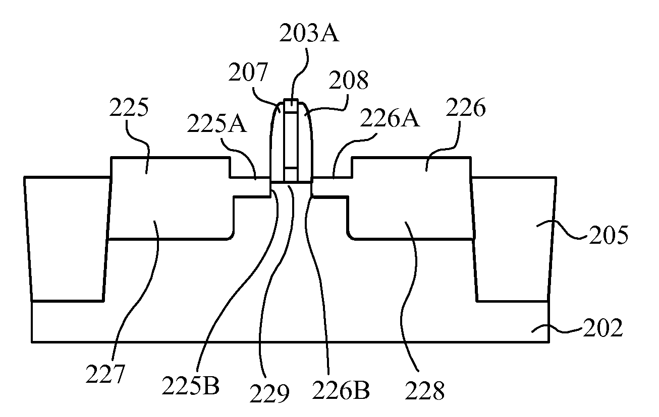
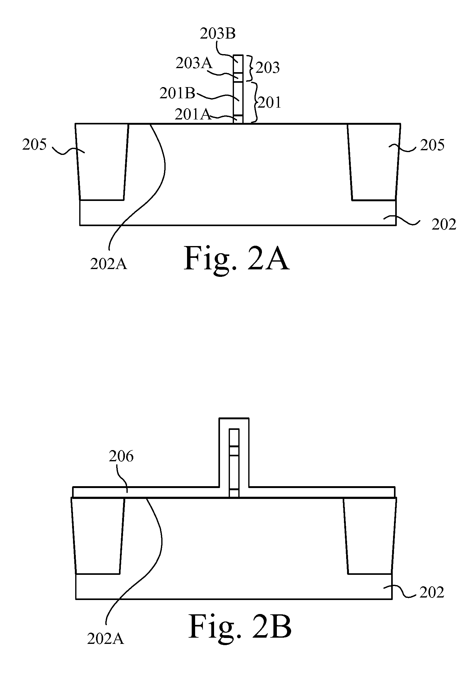
[0038]FIGS. 2A to 2L illustrate structures formed during fabrication of a strained channel transistor structure 200 (FIG. 2L) in accordance with the present invention. The final transistor structure 200 is illustrated in FIG. 2L.

[0039]FIG. 2A shows a structure having a gate structure 201 formed on a substrate 202 of a first semiconductor material which is silicon. Whilst the first semiconductor material is described here as silicon it will be understood that other materials such as germanium or GaAs or others could be used. The gate structure 201 has a gate insulating layer 201A formed on the silicon substrate 202 and a gate electrode 201B formed above the gate insulator layer 201A.

[0040]The gate insulator layer 201A is silicon oxide but it will be appreciated that other materials could be used such as silicon nitride, aluminium oxide, hafnium oxide or others alone or in combination, for example a combination of layers of silicon oxide and silicon nitride. Silicon oxide may be grown...

second embodiment

[0084]FIGS. 3A to 3H illustrate structures formed during fabrication of a strained channel transistor structure 300 in accordance with the present invention. The final transistor structure 300 is illustrated in FIG. 3H.

[0085]FIG. 3A shows a device structure having a gate structure 301 formed on a substrate 302 of a first semiconductor material which is silicon. Whilst the first semiconductor material is described here as silicon it will be understood that other materials such as germanium or GaAs or others could be used. The gate structure 301 has a gate insulating layer 301A formed on the silicon substrate 302 and a gate electrode 301B formed above the gate insulator layer 301A.

[0086]The gate insulator layer 301A is silicon oxide but it will be appreciated that other materials could be used such as silicon nitride, aluminium oxide, hafnium oxide or others alone or in combination, for example a combination of layers of silicon oxide and silicon nitride. Silicon oxide may be grown by...


PUM


Abstract

The present invention relates to semiconductor integrated circuits. More particularly, but not exclusively, the invention relates to strained channel complimentary metal oxide semiconductor (CMOS) transistor structures and fabrication methods thereof. A strained channel CMOS transistor structure comprises a source stressor region comprising a source extension stressor region; and a drain stressor region comprising a drain extension stressor region; wherein a strained channel region is formed between the source extension stressor region and the drain extension stressor region, a width of said channel region being defined by adjacent ends of said extension stressor regions.

Description

CROSS-REFERENCE TO RELATED APPLICATION(S)[0001]The present application contains subject matter related to a concurrently filed U.S. patent application Ser. No. 11 / 383,952 by Yung Fu Chong, et al. entitled “METHOD OF FABRICATING A TRANSISTOR STRUCTURE”. The related application is assigned to Chartered Semiconductor Manufacturing Ltd. and International Business Machines Corporation.FIELD OF THE INVENTION[0002]The present invention relates to semiconductor integrated circuits. More particularly, but not exclusively, the invention relates to strained channel complimentary metal oxide semiconductor (CMOS) transistor structures and fabrication methods thereof.DESCRIPTION OF THE RELATED ART[0003]Integrated circuits comprising many thousands of semiconductor devices play an important role in a number of technology areas. The continued development of devices with higher performance at reasonable cost is important to the future development of many of these technologies. Metal oxide semiconduc...

Claims


Application Information

Patent Timeline
Patent Type & Authority Patents(United States)
IPC IPC(8): H01L21/336
CPCH01L29/66628H01L29/6653H01L29/66545H01L29/6656H01L29/66636
Inventor CHONG, YUNG FULUO, ZHIJIONGHOLT, JUDSON
Owner TAIWAN SEMICON MFG CO LTD
Learn More