Method of fabricating a transistor structure

a transistor and structure technology, applied in the field of semiconductor integrated circuits, can solve the problems of difficult control, difficult to achieve in practice, and breakdown conditions, and achieve the effects of improving short channel behaviour, reducing the strain in the channel, and improving the short channel behaviour

Active Publication Date: 2007-11-22
IBM CORP
View PDF3 Cites 23 Cited by
  • Summary
  • Abstract
  • Description
  • Claims
  • Application Information

AI Technical Summary

Benefits of technology

[0027]According to a first aspect of the present invention there is provided a method of forming a strained channel transistor structure on a substrate, comprising the steps of: forming a source stressor recess comprising a deep source recess and a source extension recess; forming a drain stressor recess comprising a deep drain recess and a drain extension recess; and subsequently forming a source stressor in said source recess and a drain stressor in said drain recess. Embodiments of the present invention provide a number of advantages over the prior art. In some embodiments of the present invention, the stressors are formed in the entire source / drain and source / drain extension regions. Thus, the width of the channel region is defined by adjacent ends of the extension stressor regions. This has the advantage that a level of strain in the channel may be made higher than in prior art devices where stressors are formed only in portions of the source / drain and source / drain extension regions. In other embodiments, the width of the channel region is not exactly defined by adjacent ends of the extension stressor regions, due to a blurring effect at the interface between the stressor and substrate caused by diffusion of dopants from the extension stressor regions toward the channel during a subsequent spike anneal step. Nevertheless, extension stressor regions are extremely close to the channel region.
[0028]In embodiments of the invention, the source / drain and source / drain extension stressors are formed by means of an etch process, which has the advantage that a boundary between the source / drain and source / drain extension stressors may be made highly abrupt. Highly abrupt junctions may therefore be formed between the source / drain extension stressors and the strained channel region. This feature enables improved short channel behaviour to be attained.
[0029]Furthermore, in embodiments of the invention the source / drain stressors are formed by an uninterrupted etch process and an uninterrupted epitaxy process. An advantage of using an uninterrupted process is that the fabrication process may be performed in a shorter time period and with a reduced number of process steps. Both of these factors may have substantial implications for increased process efficiency and device yield, and reduced manufacturing costs. The uninterrupted etch and uninterrupted epitaxy process disclosed by embodiments of the invention enables a source / drain recess to be formed having an extension recess that has a depth less than that of the rest of the recess. This has the advantage of improving the stress distribution in the transistor structure.

Problems solved by technology

Punchthrough occurs when the channel length of the device is sufficiently short to allow the depletion regions at the ends of the source and drain extensions to overlap, leading to a breakdown condition.
However this has proved difficult to achieve in practice.
A disadvantage of isotropic etching processes, however, is that they are difficult to control.
In addition they may be affected by microloading effects arising from nearby protective layers.
It is therefore difficult to ensure that source and drain stressor extension recesses formed by isotropic etching are of a reproducible morphology.
A further disadvantage of the prior art is that a large number of process steps are required in order to fabricate a semiconductor device.
Solutions to these problems have been long sought but prior developments have not taught or suggested any solutions and, thus, solutions to these problems have long eluded those skilled in the art.

Method used


Image

  • Method of fabricating a transistor structure
  • Method of fabricating a transistor structure
  • Method of fabricating a transistor structure

Examples


first embodiment

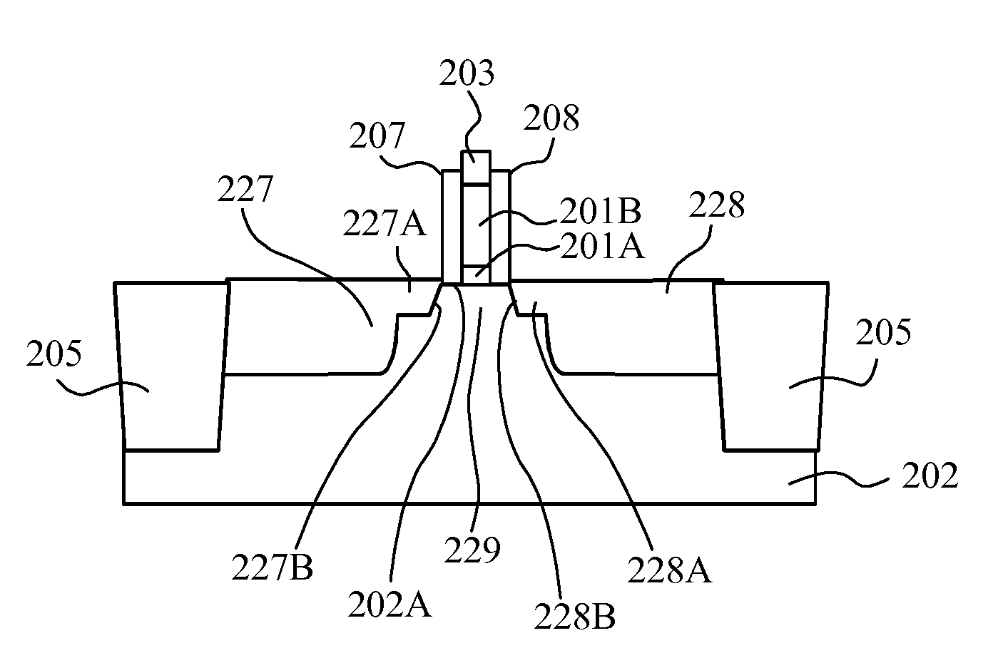
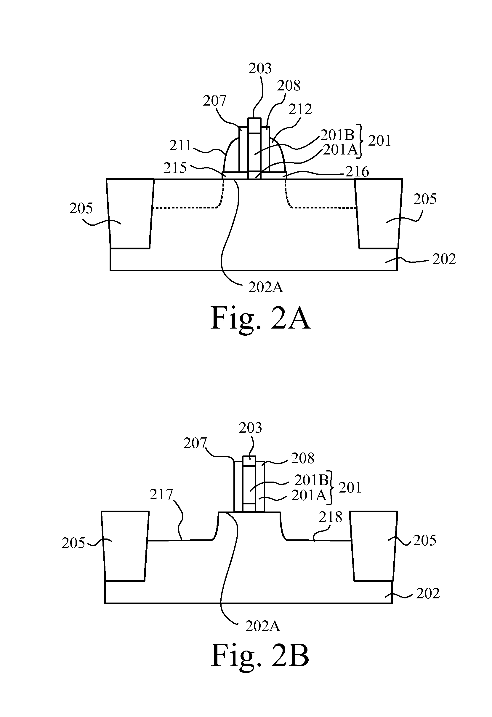
[0046]According to the invention, the disposable oxide spacer elements 215, 216 are consumed during the formation of the first portions of the deep stressor recesses 217, 218. Advantageously, parameters of the fabrication process, such as a thickness of the disposable oxide spacer elements 215, 216, the etching conditions, and other parameters are adjusted such that exposed portions of the disposable oxide spacer elements 215, 216 are entirely consumed at around the same time as formation of the first portions of the stressor recesses 217, 218 is complete. Advantageously, an etch having a low selectivity between the substrate material and the disposable oxide spacer elements 215, 216 is used.

[0047]Reactive ion etching of the source and drain stressor recesses is advantageously performed using a gaseous etchant comprising a mixture of flowing gases. The mixture of flowing gases may comprise: HBr, O2, He, Cl2, SF6, N2 (either individually or in combination) at a flow rate of from abou...

second embodiment

[0081]According to the invention, the disposable oxide spacer elements 315, 316 remain following formation of the first portions of the deep stressor recesses 317, 318. This is achieved by performing a selective reactive ion etching process. The selective reactive ion etching process is directed to etch silicon and not silicon oxide.

[0082]FIG. 3C shows the structure of FIG. 3B following the steps of removing the disposable oxide spacer elements 315, 316. The disposable oxide spacer elements 315, 316 may also be referred to as sacrificial spacer elements 315, 316.

[0083]Advantageously the disposable oxide spacer elements 315, 316 are removed by a process of reactive ion etching. Advantageously, the disposable oxide spacer elements 315, 316 are removed by changing a chemical composition of a gas from a first chemical composition, used in the reactive ion etching process used to form the first portions of the deep stressor recesses 317, 318, to a second chemical composition. Advantageou...


PUM


Abstract

The present invention relates to semiconductor integrated circuits. More particularly, but not exclusively, the invention relates to strained channel complimentary metal oxide semiconductor (CMOS) transistor structures and fabrication methods thereof. There is provided a method of forming a strained channel transistor structure on a substrate, comprising the steps of: forming a source stressor recess comprising a deep source recess and a source extension recess; forming a drain stressor recess comprising a deep drain recess and a drain extension recess; and subsequently forming a source stressor in said source stressor recess and a drain stressor in said drain stressor recess. The deep source / drain and source / drain extension stressors are formed by an uninterrupted etch process and an uninterrupted epitaxy process.

Description

CROSS-REFERENCE TO RELATED APPLICATION(S)[0001]The present application contains subject matter related to a concurrently filed U.S. patent application by Yung Fu Chong, et al. entitled “A STRAINED CHANNEL TRANSISTOR AND METHOD OF FABRICATION THEREOF”. The related application is assigned to Chartered Semiconductor Manufacturing Ltd. and International Business Machines Corporation and is identified by docket number ICIS-0230.1. FIELD OF THE INVENTION[0002]The present invention relates to semiconductor integrated circuits. More particularly, but not exclusively, the invention relates to strained channel complimentary metal oxide semiconductor (CMOS) transistor structures and fabrication methods thereof.2. DESCRIPTION OF THE RELATED ART[0003]Integrated circuits comprising many thousands of semiconductor devices play an important role in a number of technology areas. The continued development of devices with higher performance at reasonable cost is important to the future development of ...

Claims


Application Information

Patent Timeline
Patent Type & Authority Applications(United States)
IPC IPC(8): H01L21/336
CPCH01L21/3065H01L21/31116H01L29/165H01L29/7848H01L29/6659H01L29/66628H01L29/66636H01L29/6653
Inventor CHONG, YUNG FUDEZFULIAN, KEVIN K.LUO, ZHIJIONGZHU, HUILONG
Owner IBM CORP
Why Eureka
Try Eureka