Method for eliminating air bubble from photoresist and stud bump making method

A technology of photoresist and photoresist layer, which is applied in the direction of electrical components, photosensitive material processing, semiconductor/solid-state device manufacturing, etc., can solve the problems of complex process and high equipment requirements, and achieve wide application, eliminate air bubbles, and eliminate air bubbles the formation of the effect

Inactive Publication Date: 2007-11-28
SEMICON MFG INT (SHANGHAI) CORP
View PDF1 Cites 6 Cited by
  • Summary
  • Abstract
  • Description
  • Claims
  • Application Information

AI Technical Summary

Problems solved by technology

This method of eliminating bubbles in the photoresist is mainly aimed at the final photoresist packaging process, and the proces

Method used


Image

  • Method for eliminating air bubble from photoresist and stud bump making method
  • Method for eliminating air bubble from photoresist and stud bump making method
  • Method for eliminating air bubble from photoresist and stud bump making method

Examples


Example Embodiment

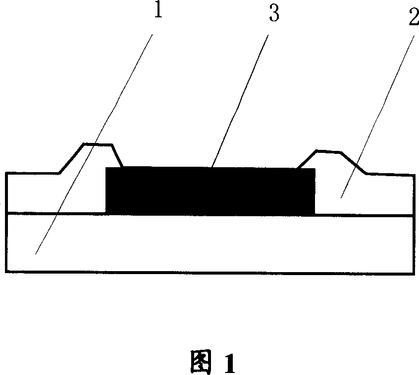
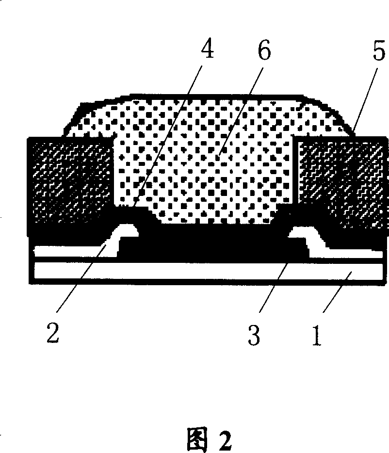
[0038] The specific embodiments of the present invention will be described in detail below with reference to the accompanying drawings. The method provided by the present invention is suitable for eliminating bubbles in the photoresist with a thickness greater than 40um, and is particularly suitable for eliminating bubbles in the photoresist during the bump manufacturing process. The method for eliminating bubbles in the photoresist of the present invention should not be limited to the bump production process. If the bubble problem of thick photoresist is involved in other manufacturing processes, the method provided by the present invention can also be well applied. In addition, the method for eliminating photoresist bubbles and the method for manufacturing bumps provided by the present invention are applicable to both wafers and chips.

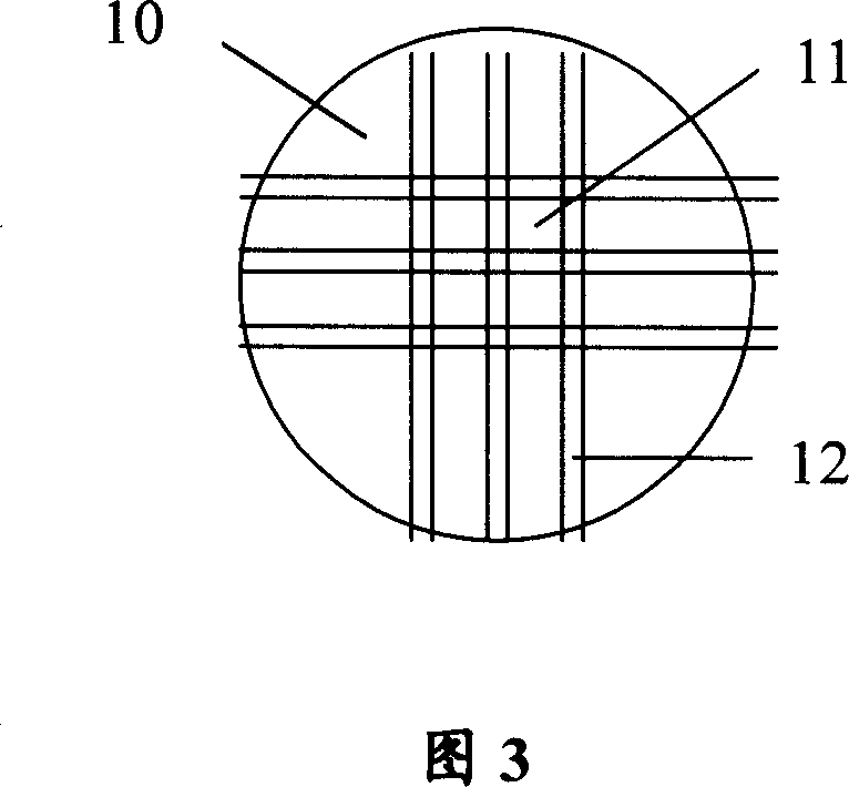
[0039] Figure 3 is a macroscopic schematic diagram of the wafer before photoresist coating; 10 represents the entire wafer, 11 represents a die...


PUM

PropertyMeasurementUnit
Thicknessaaaaaaaaaa

Abstract

The invention discloses a method to remove air bubble in photo resist, which comprises the following steps: proceeding first curing for chip; depositing sheet metal under button; forming photo resist layer; proceeding twice curing. The elimination factor of the method can reach 99.9%. This invention also relates to a producing method of button without gas bubble in photo resist to improve good product ratio in button process.

Description

technical field [0001] The invention relates to the technical field of semiconductor packaging, in particular to a method for eliminating air bubbles in photoresist before making wafer bumps and a method for making bumps. Background technique [0002] With the development of electronic products in the direction of light, thin, short, small and multifunctional, new requirements are constantly put forward for electronic packaging technology. Bump making technology (bump) is a key technology in wafer (wafer) packaging. Before the bump manufacturing process, as shown in Figure 1, the wafer 1 has completed the passivation layer 2 and the interconnection metal layer 3 process, after entering the bump manufacturing process, as shown in Figure 2, it is necessary to form a sub-bump on the wafer surface Metal layer 4 (Under-Bump Metallurgy, UBM); then a photoresist layer 5 is formed on the UBM layer, and exposed, developed to form the required bump pattern; then the bump solder 6 is ...

Claims


Application Information

Patent Timeline
IPC IPC(8): G03F7/26H01L21/00
Inventor 梅娜王津洲
Owner SEMICON MFG INT (SHANGHAI) CORP
Why Eureka
Try Eureka