Semiconductor substrate processing apparatus, method, and medium

A substrate processing and semiconductor technology, applied in the field of semiconductor substrate processing devices, can solve problems such as inability to overcome uniformity changes

Inactive Publication Date: 2007-12-12
SAMSUNG ELECTRONICS CO LTD
View PDF2 Cites 0 Cited by
  • Summary
  • Abstract
  • Description
  • Claims
  • Application Information

AI Technical Summary

Problems solved by technology

However, this technique has the problem of not being able to overcome the change in uniformity due to the change in the conditions of semiconductor substrate processing.

Method used


Image

  • Semiconductor substrate processing apparatus, method, and medium
  • Semiconductor substrate processing apparatus, method, and medium
  • Semiconductor substrate processing apparatus, method, and medium

Examples


Embodiment Construction

[0043] Reference will now be made in detail to exemplary embodiments of the present invention, examples of which are shown in the accompanying drawings. Wherein, the same reference numerals denote the same elements throughout. The exemplary embodiments are described below in order to explain the present invention by referring to the figures.

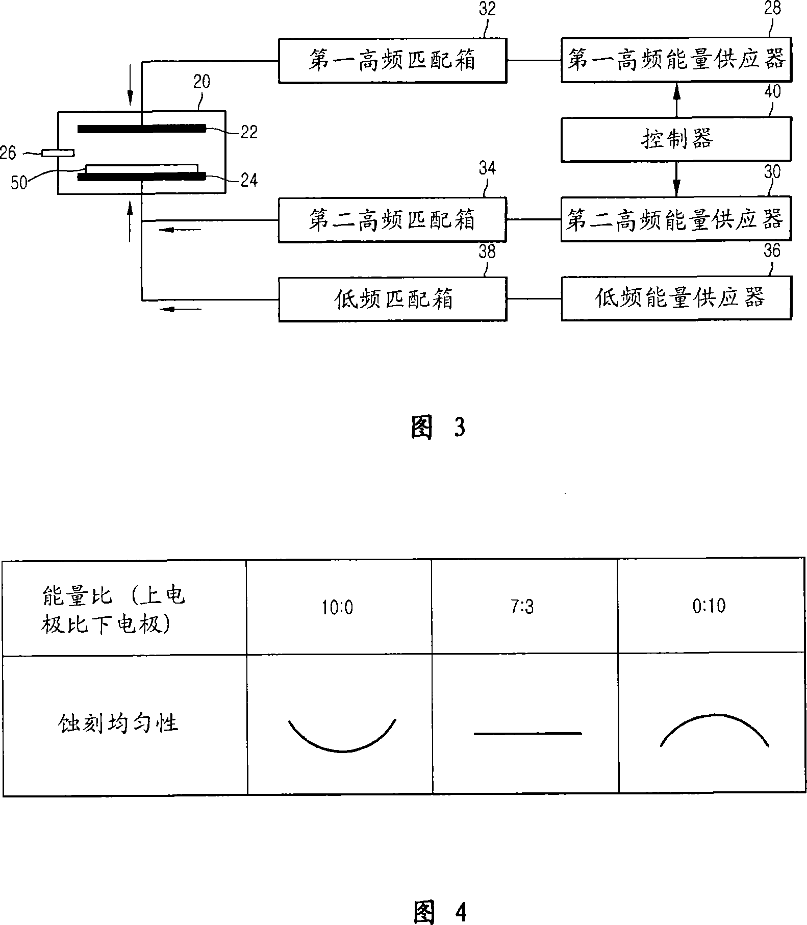
[0044] 3 is a block diagram illustrating a structure of an RF power supply system for a semiconductor substrate processing apparatus according to an exemplary embodiment of the present invention.

[0045] Referring to FIG. 3 , a semiconductor substrate processing apparatus according to an exemplary embodiment of the present invention includes a vacuum chamber 20 , an upper electrode 22 and a lower electrode 24 , a gas supplier 26 , an RF energy supplier, and a controller 40 .

[0046] The vacuum chamber 20 is a processing chamber in which semiconductor manufacturing processing is performed by plasma. In the vacuum chamber 20 , the supp...


PUM


Abstract

A semiconductor substrate processing apparatus can supply RF powers having the same frequency to upper and lower electrodes serving to generate different degrees of uniformity, and control a power ratio of the RF powers, thereby enhancing a processing uniformity of a semiconductor substrate. The apparatus includes a vacuum chamber to receive a semiconductor substrate, upper and lower electrodes disposed within the vacuum chamber, RF power suppliers to supply RF powers having the same frequency to the upper and lower electrodes, and a controller to control a power ratio of the RF powers supplied from the RF power suppliers to the upper and lower electrodes.

Description

technical field [0001] The present invention relates to an etching and deposition process in a semiconductor manufacturing process using plasma, more specifically, the present invention relates to a semiconductor substrate processing device, method and medium, the present invention can enhance the uniformity of the processing plasma to Control etch uniformity. Background technique [0002] Generally, a semiconductor manufacturing process includes a plasma etching or deposition process in which a semiconductor substrate as a target substrate is etched or deposited by plasma. Among various plasma etching devices or plasma deposition devices, a planar type inductively coupled plasma processing device is generally used. [0003] A planar type inductively coupled plasma processing apparatus includes a pair of planar electrodes (upper and lower electrodes) placed in parallel in a vacuum chamber so that processing gas is supplied into the vacuum chamber by applying RF (Radio Frequ...

Claims


Application Information

Patent Timeline
Patent Type & Authority Applications(China)
IPC IPC(8): H01L21/00H01L21/67H01J37/32H01J37/00H05H1/00H05H1/02H05H1/46
CPCH01J37/32183H01J37/32165H01J37/32091
Inventor 金明云韩文炯
Owner SAMSUNG ELECTRONICS CO LTD
Why Eureka
Try Eureka