Multilayered printed wiring board and method for manufacturing the same

A technology of wiring boards and wiring substrates, applied in multilayer circuit manufacturing, printed circuit manufacturing, container manufacturing machinery, etc.

Inactive Publication Date: 2008-01-30
DAI NIPPON PRINTING CO LTD
View PDF2 Cites 8 Cited by
  • Summary
  • Abstract
  • Description
  • Claims
  • Application Information

AI Technical Summary

Problems solved by technology

[0006] However, the rigid-flexible wiring board shown in Patent Document 1 is excellent in that it is easy to provide a substrate having both rigidity and flexibility with a high material yield, but if the electrical / flexible wiring board mounted on the surface of the substrate is not reduced, Electronic components, the substrate cannot be further miniaturized

Method used


Image

  • Multilayered printed wiring board and method for manufacturing the same
  • Multilayered printed wiring board and method for manufacturing the same
  • Multilayered printed wiring board and method for manufacturing the same

Examples


Embodiment Construction

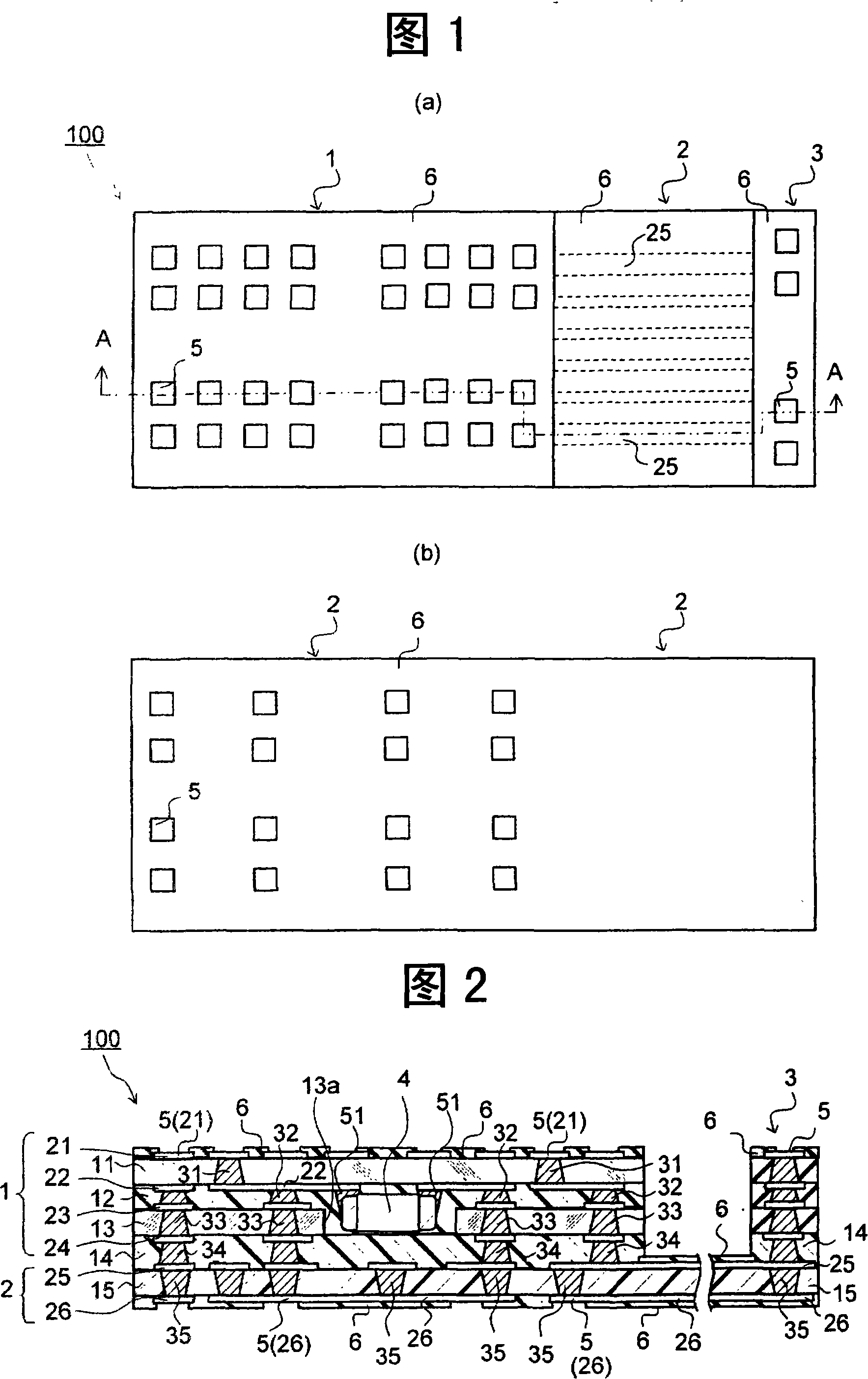
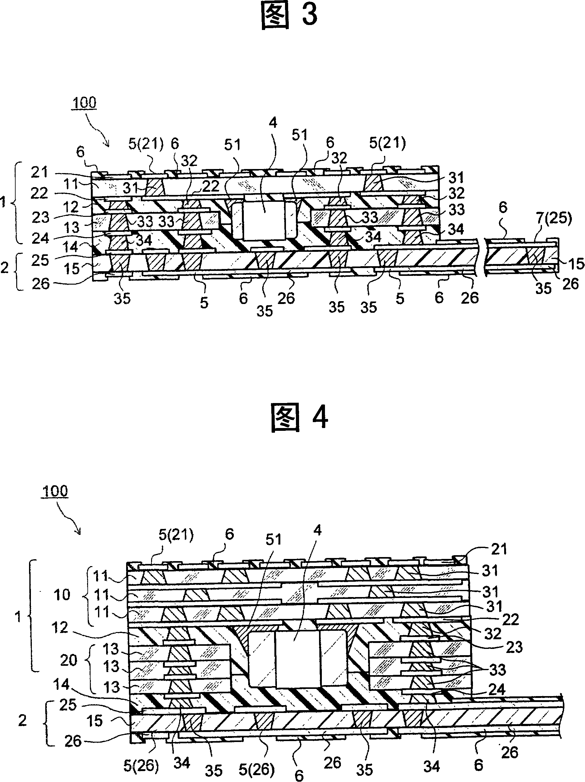
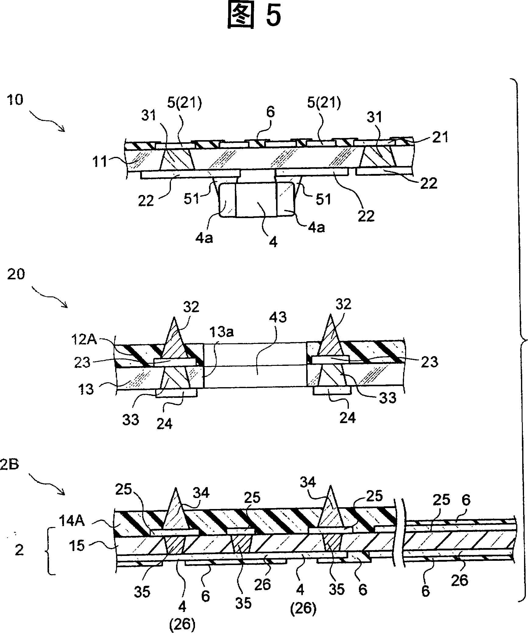
[0031] Embodiments of the present invention will be described with reference to the drawings. Hereinafter, the same reference numerals are assigned to the same or equivalent components as a principle, and descriptions thereof are omitted. Moreover, although embodiment of this invention is described based on drawings, these drawings are provided for illustration, and this invention is not limited to these drawings. In addition, each figure is schematic, and therefore the reduction ratio of each part is not necessarily the same.

[0032] First, a multilayer printed wiring board according to an embodiment of the present invention will be described based on FIGS. 1 to 4 . FIG. 1( a ) is a plan view of the multilayer printed wiring board, and FIG. 1( b ) is a bottom view (bottom view) of the multilayer printed wiring board. Fig. 2 is a schematic sectional view taken along line A-A of Fig. 1 . 3 is a schematic cross-sectional view showing a modified example of the multilayer prin...


PUM


Abstract

A multilayered printed wiring board includes a flexible wiring board with wiring layers on both main surfaces thereof; a rigid wiring board with wiring layers on both main surfaces thereof and formed opposite to the flexible wiring board under the condition that an area of the main surface of the rigid wiring board is smaller than an area of the main surface of the flexible wiring board; and an electric/electronic component embedded in the rigid wiring board.

Description

[0001] This application is based on, and claims priority from, Japanese Priority Patent Application No. 2006-205640 filed on July 28, 2006, which is hereby incorporated by reference in its entirety. technical field [0002] The present invention relates to a multilayer printed wiring board, and relates to a multilayer printed wiring board used, for example, as a module substrate in a portable device and a method of manufacturing the same. Background technique [0003] In recent years, miniaturization, weight reduction, higher functionality, and multi-combination of portable devices represented by, for example, cellular phones have progressed. Accordingly, in addition to further miniaturization, thinning, and high density, multilayer printed wiring boards used as module substrates in portable devices are also required to obtain rigidity of a predetermined strength and to be able to bend and arrange them. The degree of softness (flexibility) in a narrow case. [0004] Rigid-f...

Claims


Application Information

Patent Timeline
Patent Type & Authority Applications(China)
IPC IPC(8): H05K1/18H05K1/14H05K3/46B31B50/62
CPCH05K2203/061H05K2203/063H05K3/4647H05K3/4614H05K3/4691H05K2201/10636H05K3/4069H05K1/186Y10T29/49126Y02P70/50H05K3/46
Inventor 佐原隆广小林厚志伊贺上真左彦竹内清
Owner DAI NIPPON PRINTING CO LTD
Why Eureka
Try Eureka