Device and method for optical resizing

A technology for adjusting device and size, applied in the field of optics

Inactive Publication Date: 2008-02-13
OMS DISPLAYS LTD
View PDF13 Cites 2 Cited by
  • Summary
  • Abstract
  • Description
  • Claims
  • Application Information

AI Technical Summary

Problems solved by technology

Although simpler fabrication methods are also taught by Kawashima et

Method used


Image

  • Device and method for optical resizing
  • Device and method for optical resizing
  • Device and method for optical resizing

Examples


example 1

[0294] Optical Loss Optimization

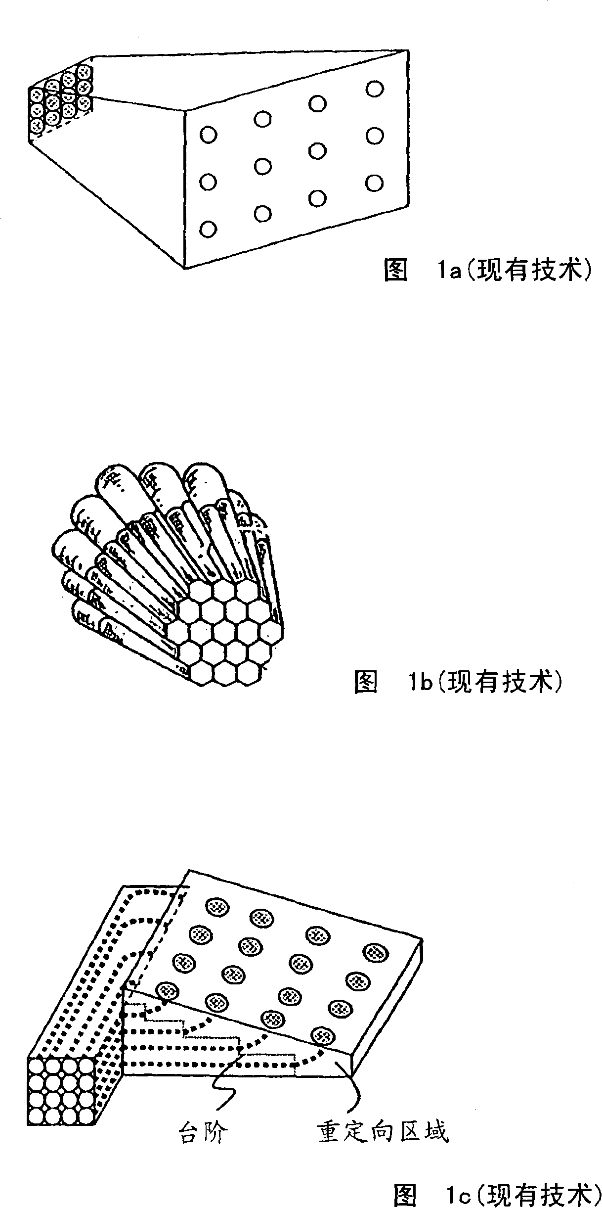
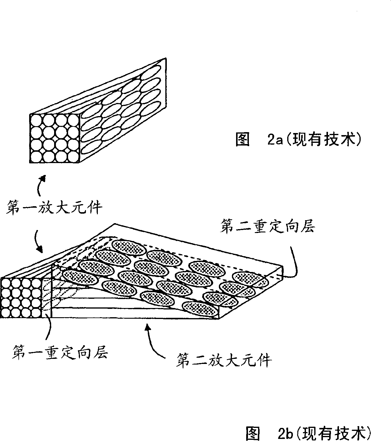
[0295]The transparency of the device is affected by several loss mechanisms: (i) propagation loss in the device; (ii) bending and tapering loss in the device; (iii) coupling loss between the optical elements of the device; and (iv) at the interface reflection loss.

[0296] For polymeric waveguides, the lowest reported propagation was obtained using polymethylmethacrylate (PMMA) and deuterated polyfluoromethacrylate (d-PFMA) materials that do not contain C–H vibration-absorbing bonds. loss. In the visible region, values ​​below 0.001 dB / cm have been reported for bulk materials [L. Hornak, "Polymers for lightwave and integrated optics," Marcel Dekker, Inc, 1992]; at λ = 0.68 μm wavelength Next, for multimode waveguides, 0.01dB / cm is reported [Yoshimura et al., "Low loss polymeric optical waveguides fabricated with Deuterated Polyfluoromethcrylate," J.Lightwave Tech, vol16, 1030-1037, 1998], and for singlemode waveguides, At wavelength λ = 1...

example 2

[0309] Field of view optimization

[0310] According to a preferred embodiment of the present invention, device 30 is designed and constructed to provide sized light at a predetermined field of view. One way to achieve a predetermined field of view for device 30 is to judiciously choose waveguide parameters for the optical elements from which device 30 outputs light (eg, element 34 ). According to a preferred embodiment of the present invention, the waveguide refractive index and numerical aperture (N.A.) are selected to satisfy the formula: N.A.=sinα=√(n 1 2 -n 2 2 ), where n 1 and n 2 are the refractive indices of the core and cladding, and α is half the diffraction angle. For a waveguide terminated in a linear taper, the effective numerical aperture is N.A / M, where M is the tapering magnification [Peli et al., supra]. In this way, an effective field of view can be selected by adjusting the taper shape, ie using a non-linear taper shape. In particular, different fiel...


PUM


Abstract

An optical resizing device is disclosed. The device comprises a plurality of layers forming a substrate having a first facet and a second facet. Each layer of the plurality of layers having an arrangement of waveguides formed and/or embedded in the layer. In one embodiment, the layers are arranged in a partially overlapping optical arrangement such that each layer has an optically exposed region at the second facet. In another embodiment, the device comprises two optical resizing elements, each configured to provide optical expansion or contraction in one dimension, such that light propagating the device experiences two-dimensional optical resizing.

Description

technical field [0001] The present invention relates to optics, and more particularly, to devices and methods for optical resizing. Background technique [0002] Miniaturization of electronic devices has been an ongoing goal in the field of electronics. Electronic devices are often equipped with some form of display that is visible to the user. As the size of these devices decreases, their display sizes also decrease. However, beyond a certain size, the display of the electronic device cannot be seen by the naked eye, and its image needs to be enlarged. [0003] The electronic display can provide a real image or a virtual image, the size of the real image is determined by the physical size of the display device, and the size of the virtual image can expand the size of the display device. [0004] Magnification of images produced by small-scale image display systems can be achieved by projecting the image onto a larger screen, or by providing a magnified virtual image to t...

Claims


Application Information

Patent Timeline
IPC IPC(8): G02B6/06
CPCG02B6/08G02B2006/12195G02B6/06
Inventor Y·沙尼
Owner OMS DISPLAYS LTD
Why Eureka
Try Eureka