Lead frame for an optical semiconductor device, optical semiconductor device using the same, and manufacturing method for these

A technology of an optical semiconductor device and a manufacturing method, which is applied in the manufacturing of semiconductor/solid-state devices, semiconductor devices, semiconductor/solid-state device components, etc., can solve the problem of not being able to obtain the luminous brightness of the optical semiconductor device, and achieve the effect of excellent luminous brightness

Inactive Publication Date: 2008-04-09
PANASONIC CORP
View PDF1 Cites 19 Cited by
  • Summary
  • Abstract
  • Description
  • Claims
  • Application Information

AI Technical Summary

Problems solved by technology

Therefore, there is a possibility that sufficient emission luminance as an optical semiconductor device cannot be obtained.

Method used


Image

  • Lead frame for an optical semiconductor device, optical semiconductor device using the same, and manufacturing method for these
  • Lead frame for an optical semiconductor device, optical semiconductor device using the same, and manufacturing method for these
  • Lead frame for an optical semiconductor device, optical semiconductor device using the same, and manufacturing method for these

Examples


Embodiment approach 1

[0047]

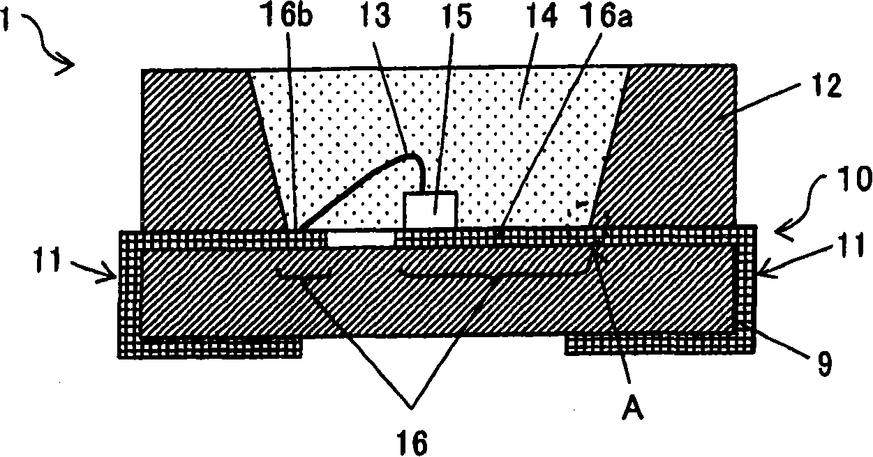
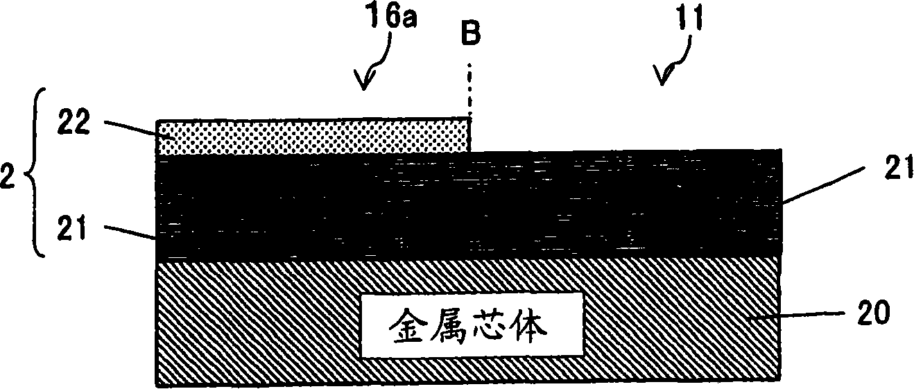
[0048] figure 1 It is a schematic cross-sectional view of the optical semiconductor device 1 according to Embodiment 1 of the present invention. figure 2 It is a schematic cross-sectional view of the lead frame 10 obtained by enlarging the vicinity of the region corresponding to the region A of the semiconductor device. figure 2 A dotted line B in , indicates the interface between the feed lead area 16 a and the external connection lead area 11 .

[0049] figure 1 The illustrated optical semiconductor device 1 is configured by disposing a lead frame 10 , peripheral resin 12 , Au wires 13 for electrical connection, sealing resin 14 , light emitting elements 15 , etc. on a substrate 9 .

[0050] Such as figure 2 As shown, the lead frame 10 has a basic structure in which a pure Ag plating layer 21 with a thickness of 1.5 μm or more is applied on the surface of a plate-shaped metal core 20 having excellent conductivity such as Cu, Cu alloy, Fe, and Fe alloy. Furt...

Embodiment approach 2

[0083]

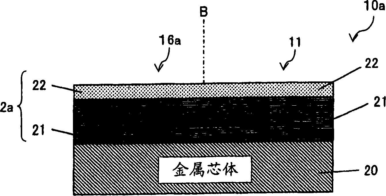
[0084] image 3 It is a partial cross-sectional schematic diagram of the lead frame 10a of the optical semiconductor device in Embodiment 2 of this invention. This part is equivalent to figure 1 The enlarged area near the area corresponding to the area in A.

[0085] This lead frame 10a is characterized in that a pure Ag plating layer 21 and an Ag—Au alloy plating layer 22 are formed on the entire surface of one surface, thereby forming a plating laminate 2a. The thicknesses of the plating layers 21 and 22 are the same as in the first embodiment.

[0086]With such a structure, the same effect as that of Embodiment 1 is exhibited. In addition, since the Ag-Au alloy plating layer 22 is coated on the entire surface of one surface of the lead frame 10a, even in the power supply lead region 16 relative to the sealing resin 14 Even when there is an error in the arrangement position, the risk of contact between the pure Ag plating layer 21 and the sealing resin 14 can b...

Embodiment approach 3

[0091]

[0092] Figure 4 It is a schematic partial cross-sectional view of the lead frame 10b of the optical semiconductor device according to Embodiment 3 of the present invention. This section is equivalent to zooming in with the figure 1 The area near the area corresponding to the A area in the middle.

[0093] This lead frame 10 b is characterized in that the Ag-Au alloy plating layer 22 having a thickness of 1.5 μm or more is directly provided on the entire surface of one side of the metal core 20 , and the pure Ag plating layer 21 is not used. The plating treatment method can be implemented in the same manner as in the second embodiment.

[0094] With such a structure, the same effect as that of Embodiment 1 can be exerted. In addition, even if the Ag-Au alloy plating layer 22 is partially peeled off or damaged in the feeder lead area 16, for example, the pure Ag component can be effectively prevented from being damaged. In contact with the sealing resin 14, excell...


PUM

PropertyMeasurementUnit
thicknessaaaaaaaaaa
thicknessaaaaaaaaaa
thicknessaaaaaaaaaa

Abstract

There is provided a lead frame for an optical semiconductor device, an optical semiconductor device using such lead frame, and a manufacturing method for these, where the optical semiconductor device exhibits favorable brightness over a long period of time by preventing discoloration and degeneration of a plating layer provide on the lead frame and a resulting reduction in a reflection coefficient for light emitted from a light emitting element, even when using silicone resin as a sealing resin. An Ag-Au alloy plating layer 22 is formed on the surface of a pure Ag plating layer 21 on a lead frame 10 sealed chloroplatinic acid-containing silicon resin, so as to prevent direct contact between the layer 21 and the silicone resin. This suppresses the formation of AgCl due to a reaction with a hardening catalyst of the silicon resin, thereby preventing the Ag plating layer from turning a blackish-brown color.

Description

technical field [0001] The present invention relates to a lead frame for an optical semiconductor device, and particularly relates to a technique for preventing deterioration of the appearance of an optical semiconductor device when it emits purple to blue light in a short wavelength region (about 400 to 500 nm). Background technique [0002] Conventionally, an optical semiconductor device using an LED element or the like as a light source has been widely used as a light source for various displays and illuminations. [0003] In this optical semiconductor device, for example, a lead frame is arranged on a substrate. After mounting a light-emitting element on the lead frame, in order to prevent deterioration of the light source or its surrounding parts caused by heat, moisture, oxidation, etc., the above-mentioned light source is sealed with a sealing resin. and its surroundings are sealed. [0004] As a material of the sealing resin, it is required to be excellent in transp...

Claims


Application Information

Patent Timeline
Patent Type & Authority Applications(China)
IPC IPC(8): H01L33/00H01L23/495H01L21/48H01L33/56H01L33/60H01L33/62
CPCH01L2924/01019H01L2924/01046H01L33/486H01L2924/01078H01L2224/45144H01L2924/01079H01L33/60H01L2224/48091H01L33/62H01L2224/48247H01L2224/48227H01L2924/12044Y10T29/49121H01L2924/00014H01L2924/00
Inventor 山田智行二神友洋河野惠志郎
Owner PANASONIC CORP
Why Eureka
Try Eureka