Integrated circuit tester

A technology for detection devices and integrated circuits, applied in the field of detection devices and detection devices for integrated circuits, can solve problems such as low scanning resolution, inability to fine-tune, and limited range of one-time detection, so as to improve scanning resolution and implementation effect Good results

Inactive Publication Date: 2008-04-23
苏州均华精密机械有限公司
View PDF0 Cites 19 Cited by
  • Summary
  • Abstract
  • Description
  • Claims
  • Application Information

AI Technical Summary

Problems solved by technology

Visual inspection is a commonly used method in the market at present, and the inspection head is fixed, so the scope of one-time inspection is limited
That is to say, if all integrated circuit products are to be inspected, they must be divided into multiple segments, which affects the output speed of laser typewriters; and the scanning resolution is not high, and fine-tuning cannot be realized according to the type of inspected products.
In addition, such facilities cannot detect the appearance defects of products well, and the same detection device can only be adapted to the same type of integrated circuit

Method used


Image

  • Integrated circuit tester
  • Integrated circuit tester
  • Integrated circuit tester

Examples


Embodiment Construction

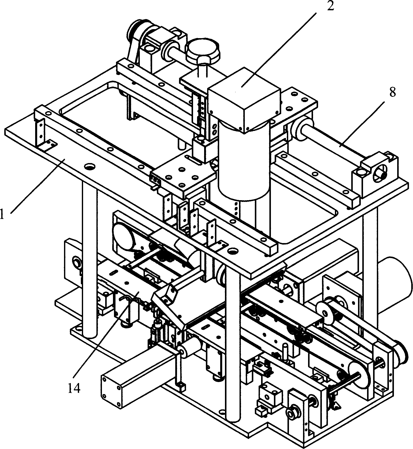
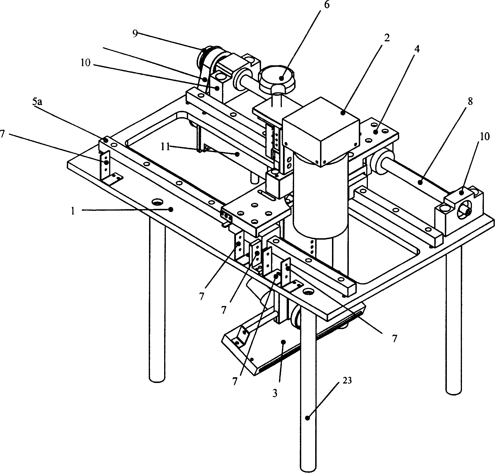
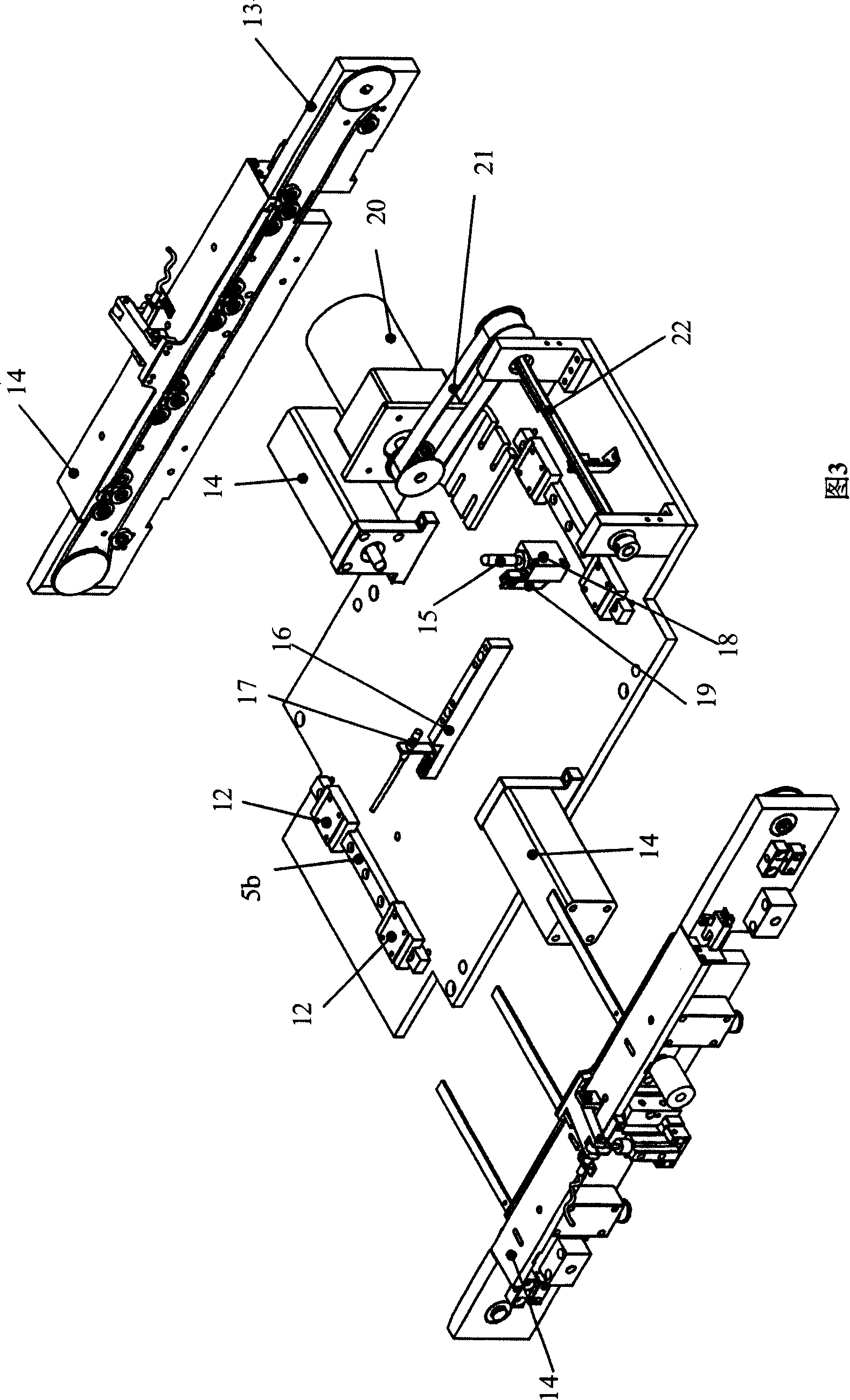
[0023] Such as figure 1 The integrated circuit detection device shown in ~3 includes a substrate, which is characterized in that: a sliding platform 1 and a positioning device are provided on the substrate, and the sliding platform 1 is equipped with a visual detection device by a connecting piece, and the positioning device includes a clamping mechanism 14, which The width of the center is adjustable, and at the same time, lifting can be realized. The visual inspection device, the sliding platform 1, and the positioning device are each driven by a driving source. Holding mechanism 14 realizes opening and closing, lifting. The connecting piece is a pillar 23, which is connected with the visual inspection device through the hole of the sliding platform 1 on the base plate.

[0024] The visual detection device includes a movable detection head 2 and an ion blower 3. There is a support block on the movable detection head 2, and a linear slide rail 5a, 5b seat 4 is arranged on th...


PUM


Abstract

On a baseboard, a sliding platform and a positioning device are set up; a vision detection device is mounted on the sliding platform via a connecting piece; said positioning device comprises a clamp assembly whose central width can be adjusted and whose height can raise up or fall down; the vision detection device, sliding platform and positioning device are respectively driven by a driven source; the driven source drive the movable detection head in the vision detection device and the clamp assembly to move.

Description

technical field [0001] The invention relates to a detection device, especially a detection device for integrated circuits, especially a detection device for the printing quality of integrated circuits after laser marking and surface defects of integrated circuits, and belongs to the technical field of integrated circuit manufacturing. Background technique [0002] In the process of integrated circuit manufacturing, laser marking is usually used, and an inspection system is required to confirm the quality of laser marking and detect surface defects of the original integrated circuit. Visual inspection is a commonly used method in the market at present, and the detection head is fixed, so the scope of one-time inspection is limited. That is to say, if all integrated circuit products are to be inspected, they must be divided into multiple sections, which affects the output speed of laser typewriters; and the scanning resolution is not high, and fine-tuning cannot be realized ac...

Claims


Application Information

Patent Timeline
Patent Type & Authority Applications(China)
IPC IPC(8): G01N21/898H01L21/66G01R31/26
Inventor 周文进陈峰
Owner 苏州均华精密机械有限公司
Why Eureka
Try Eureka