Light-emitting panel for illuminating or displaying images provided with a composite transparent upper electrode

A technology for image display panel and electroluminescent layer, which is applied in the direction of installation/support/configuration/insulation of electroluminescent light source, electrode assembly, electric light source, etc., and can solve problems such as unfavorable luminous efficiency and loss of transparency of the upper electrode

Active Publication Date: 2008-05-14
INTERDIGITAL CE PATENT HLDG
View PDF5 Cites 2 Cited by
  • Summary
  • Abstract
  • Description
  • Claims
  • Application Information

AI Technical Summary

Problems solved by technology

[0008] Document WO2004/049465 states that this metal buffer layer must be of sufficient thickness (>30nm) to achieve effective protectio

Method used


Image

  • Light-emitting panel for illuminating or displaying images provided with a composite transparent upper electrode

Examples


Example Embodiment

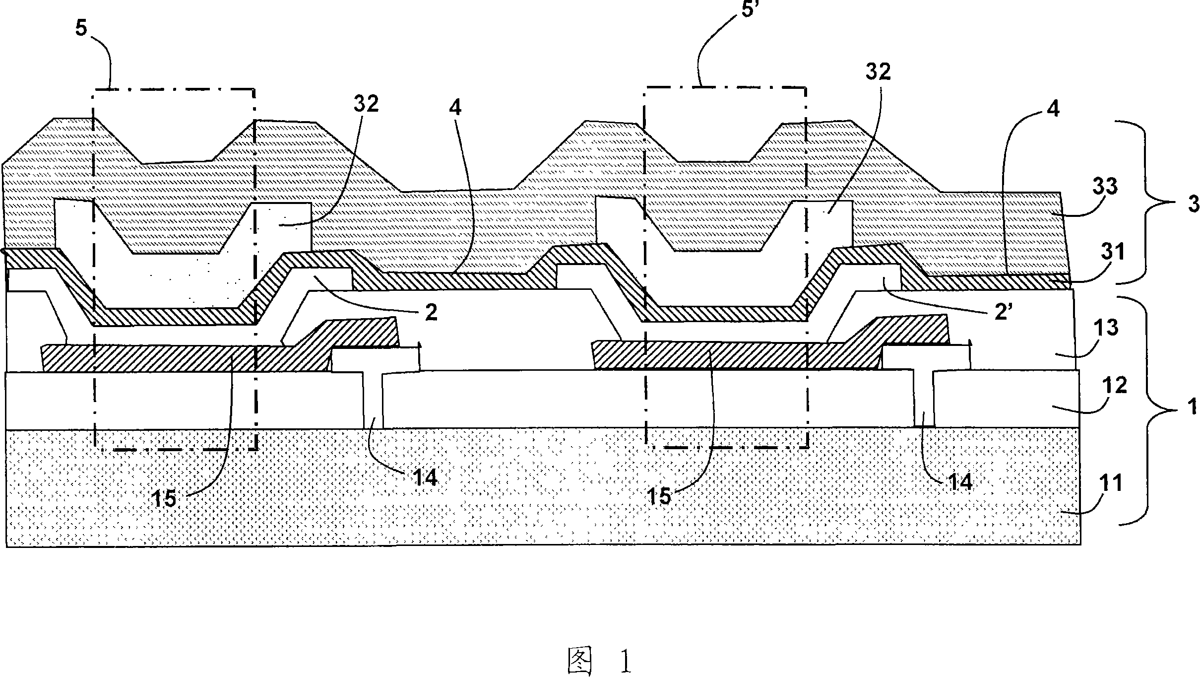
[0030]The structure starts with a substrate 1 incorporating here the known active matrix, the manufacture of which will not be described in detail here: a rigid plate 11 made of insulating material supports the so-called "pixel circuit" for the diodes. A network of control / supply circuits, each having an output 14 connected to a lower electrode 15, which is preferably metallic and reflective. This rigid plate generally supports several electrically insulating layers, including a first insulating layer 12 for isolating the components of the pixel circuit from each other in particular and a second insulating layer 12 for separating the diodes and isolating the lower electrode from the upper electrode outside the emitting area of ​​the diode. Two insulating layers 13 . At the position of the diode, this second insulating layer 13 is penetrated by a window, exposing the surface of the lower electrode 15 . Finally, the substrate integrates a further array (not shown) of electrodes...


PUM

PropertyMeasurementUnit
Thicknessaaaaaaaaaa
Thicknessaaaaaaaaaa

Abstract

The invention concerns a panel whereof at least one of the upper electrodes is common to a plurality of diodes (5, 5') and comprises a first conductive layer (31) and a second conductive layer (33), and an isolating and transparent buffer layer (32) which is interposed between said two conductive layers (31, 33) and which is perforated with windows which provide direct contact zones (4) between the two conductive layers (31, 33) of said common electrode (3), said contact zones (4) being separated from the active zones of the diodes (5, 5'). The presence of said direct contact zones between the two conductive layers, enables a good distribution of current to be provided by the upper electrode while the intermediate buffer layer is insulating.

Description

technical field [0001] The invention relates to an illumination or image display panel comprising an array of organic light emitting diodes supported by a substrate. Background technique [0002] The prior art describes the above panels in which each diode comprises an organic electroluminescent layer sandwiched between a lower electrode contacting the substrate and an upper electrode transparent to the light emitted by the organic electroluminescent layer. So this is what is known as a "top-emitting" panel. In this case, the top electrode is either the cathode (for a "normal" diode structure) or the anode (for an "inverted" structure). [0003] In general, there are other organic layers between the electrodes, for example layers for injecting and transporting holes or electrons and / or for optimizing light extraction, especially taking advantage of resonance effects in the optical cavity between the electrodes. [0004] The prior art also describes panels in which at least...

Claims


Application Information

Patent Timeline
IPC IPC(8): H05B33/26H01J1/88G09F9/33H01L27/15
CPCH01L51/5221H01L27/3244H05B33/26H01L51/5206H10K59/12H10K50/816H10K50/828H10K2102/3026H01L31/022475H10N30/10516H10K50/13H10K50/81H10K50/82
Inventor 冈瑟·哈斯贝努瓦·拉西尼戴维·沃弗雷
Owner INTERDIGITAL CE PATENT HLDG
Why Eureka
Try Eureka