Method of detecting the relative positioning of two signals and corresponding device

Active Publication Date: 2006-03-16
STMICROELECTRONICS SRL
27 Cites 0 Cited by

AI-Extracted Technical Summary

Problems solved by technology

However, such an approach produces stability problems because one clock signal is sampled with the aid of a signal of...

Benefits of technology

[0005] For example, if one wishes to transmit information of the domain regulated by the clock having the higher frequency to the domain regulated by the clock having the lower frequency, it is preferable to perform the transmission on the first edge of the signal of the clock at high frequency corresponding to an edge of the signal of the clock at low frequency. One thus benefits from more time for performing the transmission of data, thereby limiting the risks of data loss.
[0006] A method aspect of the invention may be for detecting the relative positioning of two clock signals, one of these clock signals being a fast clock signal and the other a slow clock signal. The frequency of the fast clock may be n times greater than the frequency of the slow clock, and n is an integer greater than 1. A phase logic signal may be generated from the two clock sig...

Abstract

A device is for detecting a relative positioning of two clock signals including a fast clock signal and a slow clock signal. The fast clock frequency may be n times greater than a slow clock frequency, and n includes an integer greater than 1. The device includes a phase logic signal generator for generating a phase logic signal from the two clock signals by assigning a predetermined logic value to the phase logic signal when a rising edge of the fast clock signal matches a predetermined location of the slow clock signal.

Application Domain

Technology Topic

Image

  • Method of detecting the relative positioning of two signals and corresponding device
  • Method of detecting the relative positioning of two signals and corresponding device
  • Method of detecting the relative positioning of two signals and corresponding device

Examples

  • Experimental program(1)

Example

[0026]FIG. 1 represents two clock signals HL and HR, defining two distinct clock domains, in the case where the signal HL is twice as fast as the signal HR (n=2). Two different cases will be considered for the clock signal HL.
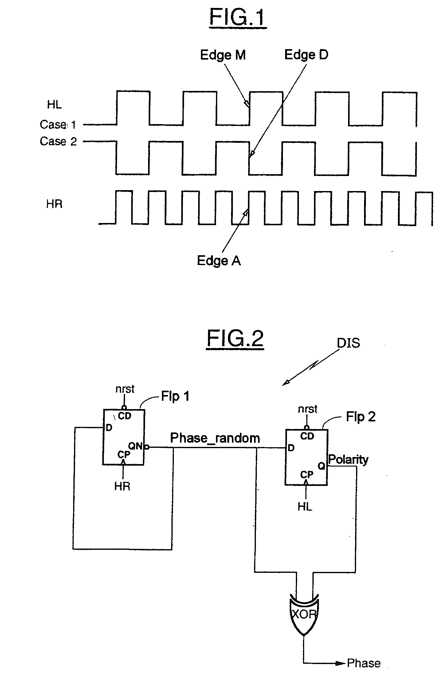
[0027] Case 1 illustrates a first configuration where the two clocks are active on edges of like polarity such that a rising edge A of the fast clock HR corresponds to a rising edge M of the slow clock HL. Case 2 illustrates another configuration where the two clocks are active on edges of opposite polarities such that a rising edge A of the fast clock HR corresponds to a falling edge D of the slow clock HL.
[0028] In the example illustrated in FIG. 1, the two clock signals HL and HR are aligned, that is to say an edge of the clock signal Edge A, corresponds to an edge of the clock signal HL. However, during the embodiment of the circuit, the technology of the electronic components used may generate a shift between the edges of the clock signals.
[0029] Furthermore, the frequency of the clock signal HR is n times higher than the frequency of the clock signal HL. In this example, n=2, however, n may be any integer greater than 1.
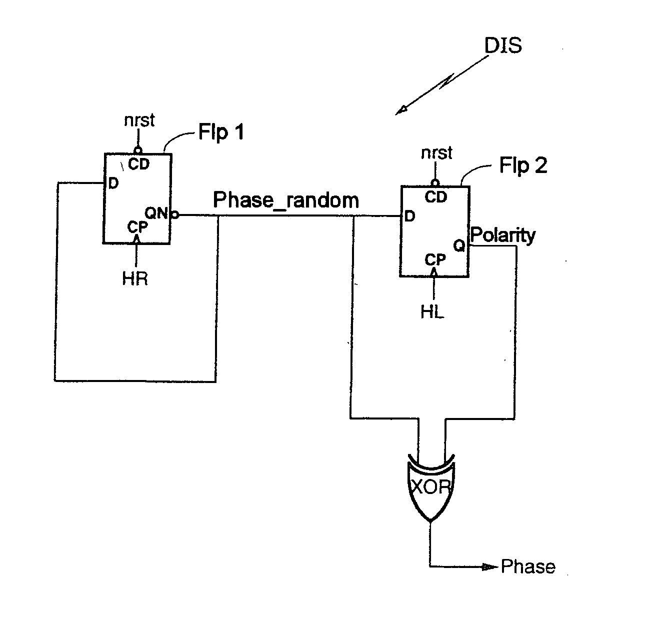
[0030] Referring now to FIG. 2, a device DIS in accordance with the invention is illustrated. The device DIS comprises a first sequential element Flp 1, which includes a flip-flop D, for example. Hereinbelow, it will be considered that the sequential elements used in the examples described are flip-flops controlled by a reset to zero signal nrst.
[0031] The flip-flop Flp 1 is regulated by the fast clock signal HR. The fast clock signal HR has the higher frequency as is represented in FIG. 1. Additionally, the output QN of the flip-flop Flp 1 is looped back to its input D. The flip-flop Flp 1 outputs a first intermediate logic signal Phase_random.
[0032] The device DIS also comprises a second sequential element Flp 2. The flip-flop Flp 2 is regulated by the slow clock signal HL, which has the lower frequency. For this device, the frequency of the fast clock HR may be twice as fast as that of the slow clock HL (n=2). The input D of the second flip-flop Flp 2 is connected to the output QN of the first flip-flop Flp 1. The second flip-flop Flp 2 therefore receives as input the intermediate logic signal Phase_random. Additionally, the second flip-flop Flp 2 delivers via its output terminal Q a second intermediate logic signal Polarity. The first and second intermediate logic signals, Phase_random and Polarity are delivered as input to an EXCLUSIVE OR logic gate, XOR. The XOR logic gate then delivers an output signal Phase, as a function of the two input signals Phase_random and Polarity.
[0033] Referring now additionally to FIG. 3 which describes the profile of these signals implemented in the device DIS of FIG. 2. The fast and slow clock signals HR and HL are the signals represented in FIG. 1. The frequency of the fast clock signal HR is, in this example, twice as high as the frequency of the slow clock signal HL.
[0034] Two cases relating to the values taken by the signal Phase_random will be considered. Case A represents the situation where the first value taken by the signal Phase_random is “0”. In this case, the signal Phase_random takes successively the values “0” and then “1”, at the frequency of the fast clock signal HR.
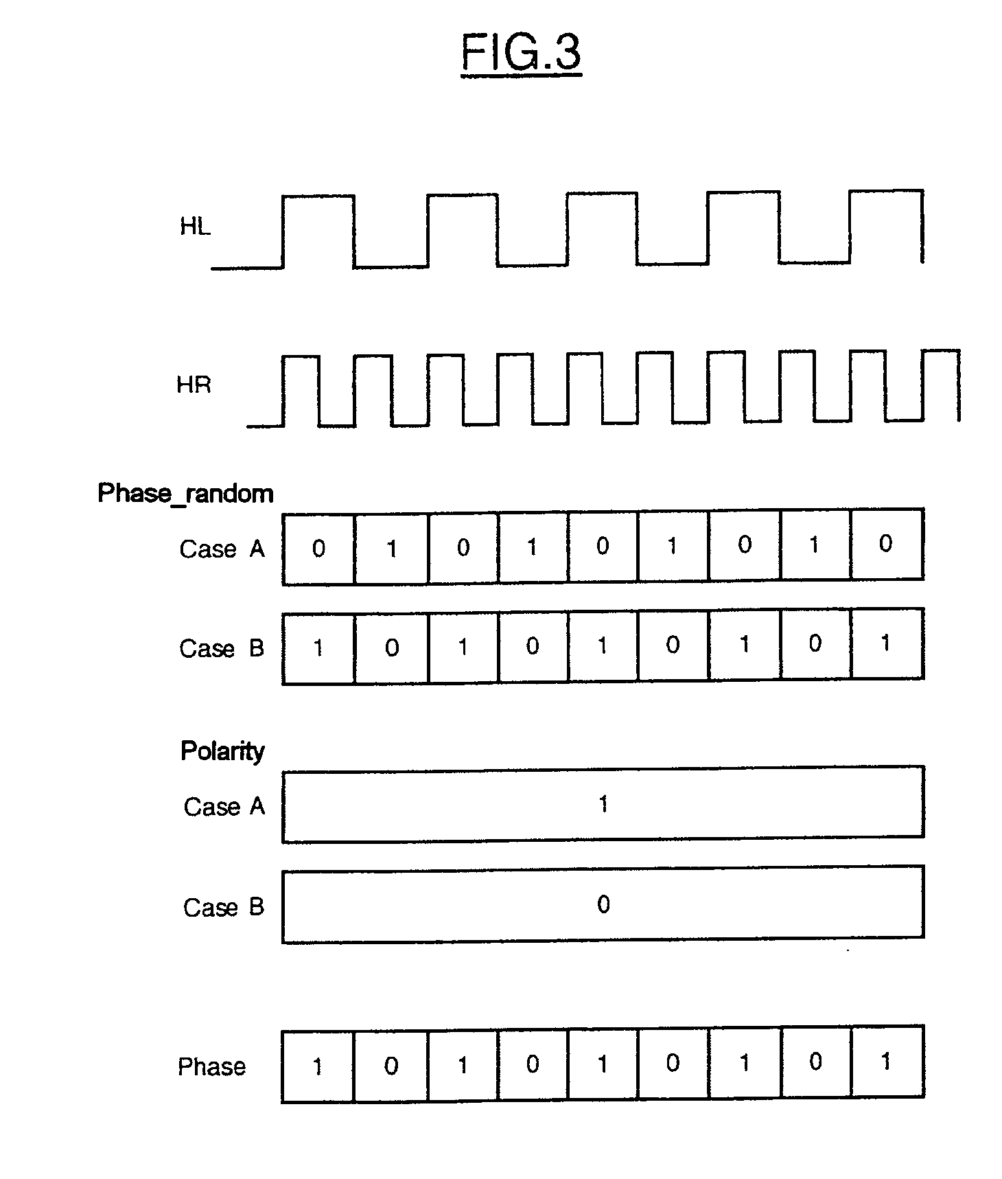
[0035] Case B represents the situation where the first value taken by the signal Phase_random is “1”. In this case, the signal Phase_random takes successively the values “1” and then “0”, at the frequency of the fast clock signal HR.
[0036] Accordingly, as the values of the signal Phase_random follow case A or case B, the signal generated by the flip-flop Flp 2, Polarity, evolves according to two cases, case A or case B. The signal Polarity evolves according to case A if the signal Phase_random evolves also according to case A. In this case, the signal Polarity takes the value “1” regardless of the value of the signal Phase_random. The signal Polarity evolves according to case B if the signal Phase_random evolves according to case B. In this case, the signal Polarity takes the value “0” regardless of the value taken by the signal Phase_random.
[0037] The signal Phase is generated by the “EXCLUSIVE OR” logic gate, XOR. It is recalled that according to the truth table of the “EXCLUSIVE OR” function, the output signal equals “1” if the two input signals are in a different state. Otherwise, the output signal equals “0” if the two input signals are in an identical state.
[0038] Thus, regardless of the case of the evolution of the values of the signals Phase_random and Polarity, case A or case B, the evolution of the signal phase is the same, that is to say it takes successively the values “1” then “0”. According to the hypotheses defined for the embodiment illustrated, the “1” logic value signifies that a rising edge of the fast clock signal HR corresponds to a rising edge of the signal of the slow clock HL.
[0039] Reference is now made to FIG. 4 which represents a variant of the device illustrated in FIG. 2, operating with any ratio n between the two clocks. The first sequential element Flp 3 of the device DIS 2 of FIG. 4 is regulated by the slow clock signal HL. The second sequential element Flp 4 is regulated by the fast clock signal HR. Thus, the role of the two sequential elements of the device DIS in FIG. 2 have been reversed.
[0040] Reference is now made to FIG. 5 which illustrates the evolution of the signals implemented in the variant represented in FIG. 4. The slow and fast clock signals HL and HR are generated such that the frequency of the fast clock signal HR is three times higher than the frequency of the slow clock signal HL, for example. The signal Phase_random may evolve according to two distinct cases.
[0041] The first case illustrates the situation where the first value taken by the signal Phase_random is “0”. In this case, the signal Phase_random takes successively the values “0” and then “1” at the frequency of the signal of the slow clock HL, which regulates the first sequential element Flp 3. If the signal Phase_random evolves according to case B, then it takes successively the values “1” and then “0” at the frequency of the clock signal HL.
[0042] Just as for the device DIS of FIG. 2, the signal Polarity evolves also according to two cases, case A and case B, respectively associated with case A and with case B of the signal Phase_random. If the signal Polarity evolves according to case A, then it takes successively the values “0” and then “1” at the frequency of the signal of the slow clock HL. Conversely, if the signal Polarity evolves according to case B, then it takes successively the values “1” and then “0” at the frequency of the signal of the slow clock HL. Thus, regardless of the case according to which the signals Phase_random and Polarity evolve, the signal Phase generated by the “EXCLUSIVE OR” logic gate XOR, takes the value “1” when a rising edge of the signal of the fast clock HR corresponds to a rising edge of the signal of the slow clock HL, or the value “0” otherwise.
[0043] A first exemplary use of the device DIS represented in FIG. 2 is illustrated in FIG. 6. In this example two clock signals are used, a first fast clock signal H_200 whose frequency is 200 MHz and a second slow clock signal H_100 whose frequency is 100 MHz.
[0044] The system SYS represents a system for synchronized transmission of data between two domains of different frequencies. An input flip-flop Flp 5 is regulated by the fast clock signal HR_200. The flip-flop Flp 5 is also controlled by a reset to zero signal nrst. The output Q of the flip-flop Flp 5 is looped back to its input D by way of a selector SEL which also receives data Data as input. Additionally, the selector SEL is controlled by a control signal which is the Phase logic signal, generated by the device DIS represented in FIG. 2. According to the value of the Phase logic signal, the selector SEL transmits the data Data to the input D of the flip-flop Flp 5. The flip-flop Flp 5 delivers data Data_s via its output Q.
[0045] The output Q of the flip-flop Flp 5 is also connected to the input D of an output flip-flop Flp 6, controlled by a reset to zero signal nrst. The flip-flop Flp 6 is regulated by the slow clock signal HL_100.
[0046] The flip-flop Flp 6 receives as input the data Data_s delivered by the output Q of the flip-flop Flp 5. Thus, by virtue of the system SYS, it is possible to check that at each clock tick of the signal of the fast clock HR, the data may be delivered so that the time available during the exchange of data is as great as possible. Stated otherwise, a cycle of n period of the faster clock signal (in this example n is equal to 2) is guaranteed so as to allow the exchange of data.
[0047] If reference is made to FIG. 7, which illustrates the signals implemented in the system SYS of FIG. 6, it is possible to see the clock signals HL_100 and HR_200, such that the frequency of the clock signal HR_200 is 200 MHz and that of the signal of the clock HL_100 is 100 MHz. The signal Phase takes successively the values “1” then “0”. When the signal Phase takes the value “1”, a rising edge of the clock signal HR_200 corresponds to a rising edge of the clock signal HL_100. Thus, the data Data_s are exchanged when a rising edge of the signal of the fast clock HR_200 corresponds to a rising edge of the clock signal HL_100.
[0048] Reference will now be made to FIG. 8. The system SYS 2 represents a second use of the device represented in FIG. 2. The system SYS 2 is a system for the controlled multiplexing of data, such as to transmit in a predetermined order coefficients representing the luminance and the blue and red chrominances of a digital video application, for example.
[0049] The system SYS 2 comprises four flip-flops Flp 8, Flp 9, Flp 10 and Flp 11 in parallel. Each of the four flip-flops is controlled by a reset to zero signal nrst and is regulated by the slow clock signal HL, which in this example is equal to 6.75 MHz. The four flip-flops Flp 8, Flp 9, Flp 10 and Flp 11 are respectively fed with the coefficients of the luminance Y0, of the blue chrominance Cb, of the red chrominance Cr and of luminance Y1. Via their output terminals Q, they deliver the data which they receive on their input terminal D as a function of the signal of the slow clock HL.
[0050] These output data are delivered to a multiplexer MUX1, controlled by a counter-modulo_4, CMP4. The counter-modulo_4 CMP4 receives on an input E_raf the logic signal Phase, delivered by the device represented in FIG. 2. The signal Phase is intended to control the refreshing of the counter-modulo_4, CMP4. As a function of the control signal COM delivered by the counter-modulo_4 CMP4, the multiplexer MUX 1 outputs in order the data Data_s corresponding to the planes Y0, Cb, Cr, and Y1.
[0051] The data Data_s are delivered on the input D of a flip-flop Flp 7. The flip-flop Flp 7 is controlled by a reset to zero signal nrst and regulated by the fast clock signal HR. In this example, the frequency of the fast clock signal is 27 MHz. The flip-flop Flp 7 delivers via its output terminal Q, the data stream YCbCr at the frequency of the signal of the fast clock HR, which is 27 MHz.
[0052] Reference is now made to FIG. 9 which represents another exemplary use of the device represented in FIG. 2. The system SYS 3 of FIG. 9 represents a system for controlled multiplexing of data. The system SYS 3 comprises a first flip-flop Flp 12 controlled by a reset to zero signal nrst and regulated by a slow clock signal HL. The flip-flop Flp 12 receives as input data Data, that it delivers via its output terminal Q to a mixer MEL. The mixer MEL also receives as input data arising from a multiplexer MUX 3. The multiplexer MUX 3 receives as input n coefficients Coeff_1, . . . , Coeff_n.
[0053] Furthermore, the multiplexer MUX 3 is controlled by an output signal arising from a modulo n counter, CMPn. The modulo n counter CMPn is regulated by the fast clock signal HR. Furthermore, it is controlled by the logic signal Phase, received on its input E_raf and able to control the refreshing of the modulo n counter, CMPn. Thus, the multiplexer MUX3 controlled by the modulo n counter CMPn, makes it possible to successively apply the n coefficients, Coeff_1, . . . , Coeff_n, to the data delivered by the flip-flop Flp 12. The application of the n coefficients is effected by way of the mixer MEL. The output signal from the mixer MEL is delivered to an adder ADD. The adder ADD may also receive as input, in parallel, other data arising from other flip-flops, for example the flip-flop Flp 13, connected in series with the flip-flop Flp 12.
[0054] The adder ADD outputs a resultant signal formulated by adding up the various data delivered as input to the adder ADD. The resultant signal delivered by the adder ADD is transmitted to an output flip-flop Flp 14 controlled by a reset to zero signal nrst and regulated by the fast clock signal HR. The flip-flop Flp 14 then outputs an output signal S at the frequency of the signal of the fast clock HR. It is noted that in this example, the frequency of the fast clock HR is n times higher than the frequency of the signal of the slow clock HL, and n being the number of coefficients delivered to the input of the multiplexer MUX3.

PUM

no PUM

Description & Claims & Application Information

We can also present the details of the Description, Claims and Application information to help users get a comprehensive understanding of the technical details of the patent, such as background art, summary of invention, brief description of drawings, description of embodiments, and other original content. On the other hand, users can also determine the specific scope of protection of the technology through the list of claims; as well as understand the changes in the life cycle of the technology with the presentation of the patent timeline. Login to view more.

Similar technology patents

Method for detecting icing and de-icing

ActiveUS20200018293A1Limit riskMinimize operationEngine fuctionsMachines/enginesPhysicsTurbine blade
Owner:ELECTRICITE DE FRANCE +2

Classification and recommendation of technical efficacy words

  • More time
  • Limit risk

System and Methods for Geographically-Driven Downstream Distribution of Mobile Content

InactiveUS20140164125A1Good effectivenessMore timeMarketingHandheld equipmentMobile media
Owner:CONTAINER MEDIA

Spacer interposed between a blade root and the bottom of a slot in the disk in which the blade is mounted

ActiveUS20090004017A1Limit impactLimit riskPropellersRotary propellersKnife bladesContact region
Owner:SN DETUDE & DE CONSTR DE MOTEURS DAVIATION S N E C M A

Device for anastomosis

InactiveUS20050228409A1Limit riskSimple and rapidSuture equipmentsBlood vesselsDistal anastomosisBiomedical engineering
Owner:G A M A H S
Why Eureka
Try Eureka