
Image sensors with output noise reduction mechanisms

An image sensor and capacitor technology, applied in image communication, color TV parts, TV system parts, etc., can solve the problems of increasing chip manufacturing costs, frame rate reduction, and unsatisfactory high-speed imaging applications of imaging devices, etc.

Active Publication Date: 2008-06-04
OMNIVISION TECH INC
View PDF0 Cites 14 Cited by
  • Summary
  • Abstract
  • Description
  • Claims
  • Application Information

AI Technical Summary

Problems solved by technology

However, there are a number of disadvantages associated with this conventional technique
First, the additional on-chip / off-chip storage required to store successive frames during processing can greatly increase the required chip area and associated manufacturing costs
Second, averaging two consecutive frames reduces the available frame rate by 50%
Therefore, imaging setups implementing this technique may not be ideal for high-speed imaging applications

Method used


Image

  • Image sensors with output noise reduction mechanisms
  • Image sensors with output noise reduction mechanisms
  • Image sensors with output noise reduction mechanisms

Examples


Embodiment Construction

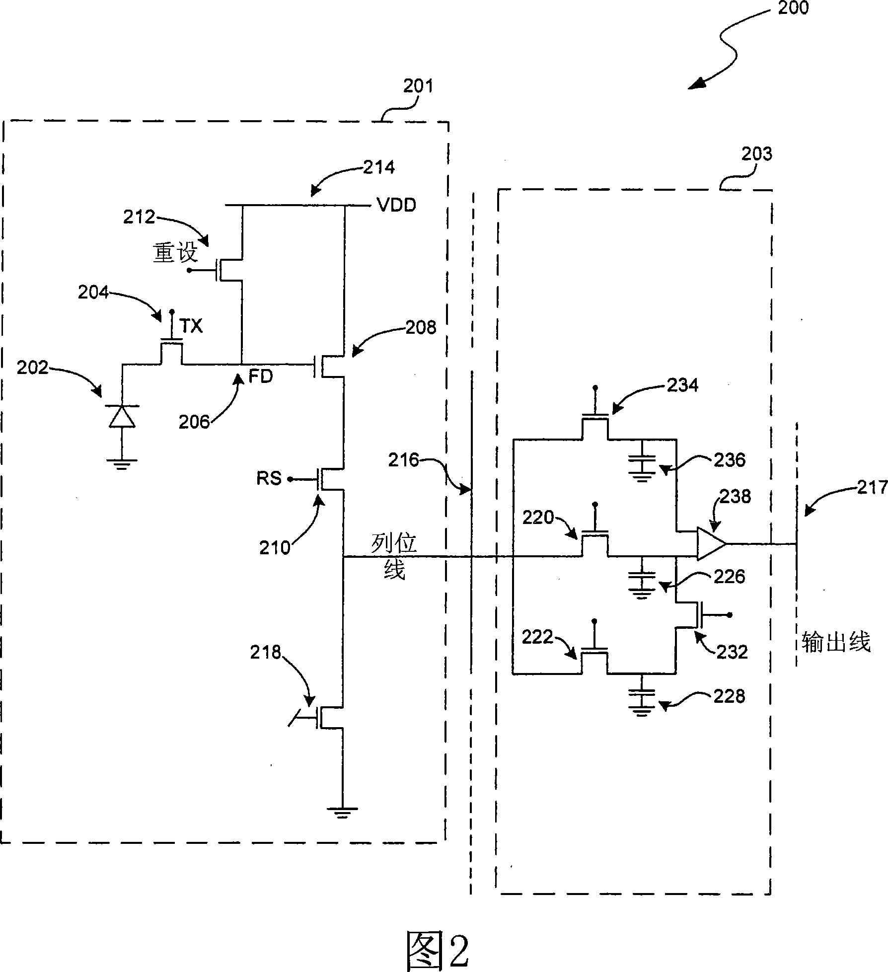
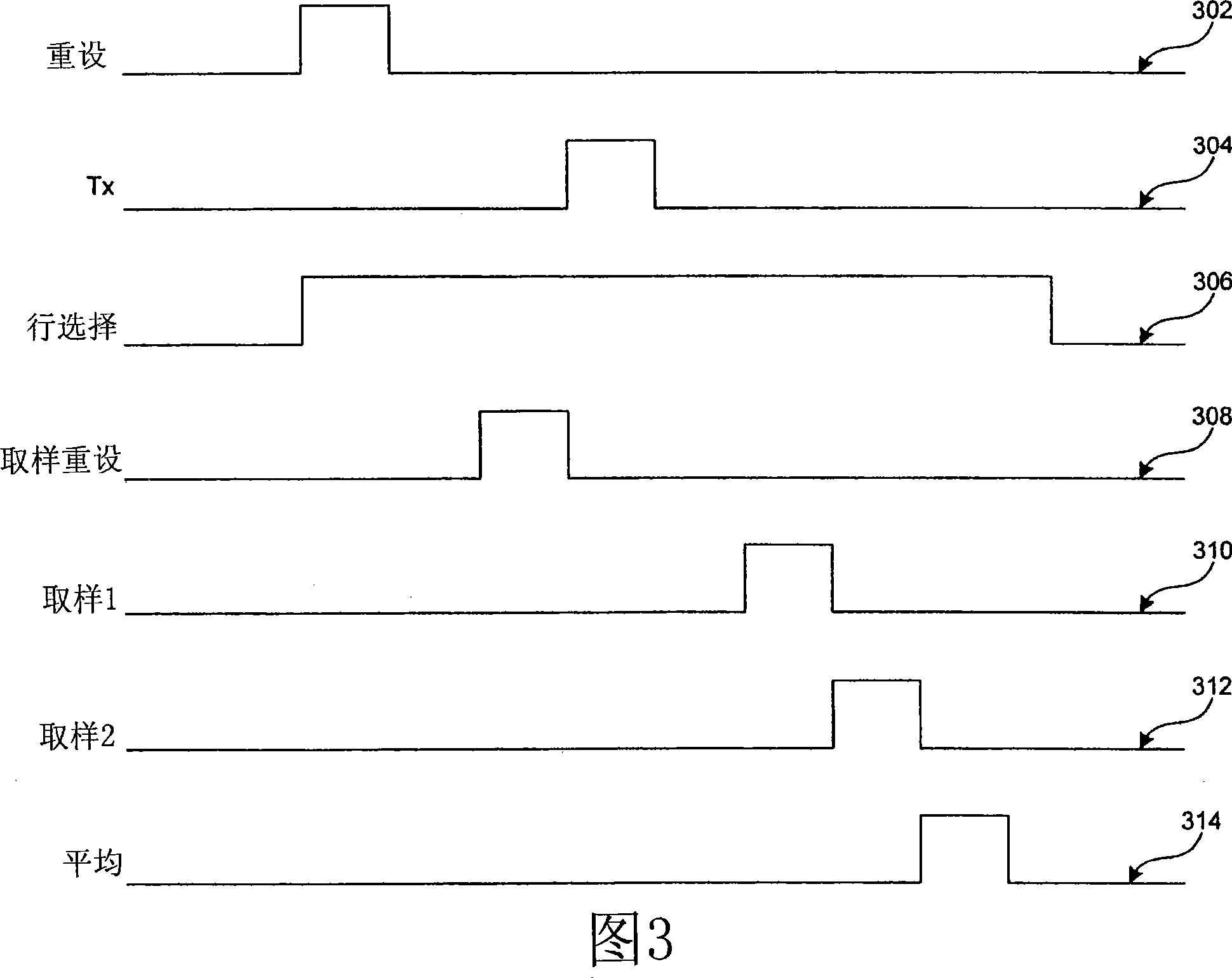
[0022] This disclosure describes image sensors with output noise reduction mechanisms. It will be appreciated that several of the details set forth below are provided to describe the following embodiments in a manner sufficient to enable a person skilled in the relevant art to make and use the disclosed embodiments. However, several of the details and advantages described below may not be necessary to practice some embodiments of the invention. In addition, the invention may include other embodiments within the scope of the claims but not described in detail with reference to FIGS. 2-6 .

[0023] FIG. 2 illustrates an image sensor 200 having an output noise reduction mechanism and configured in accordance with an embodiment of the invention. Image sensor 200 includes pixel elements 201 for converting incident light into electrical signals. The pixel element 201 includes a transfer transistor 204 that connects the light sensing element 202 to a floating node 206 . The light ...


PUM


Abstract

An image sensor having readout noise reduction mechanisms is disclosed. The image sensor can include a first sampling transistor, a second sampling transistor connected to the first sampling transistor, an averaging transistor electrically connecting the first and second sampling transistors in series, a reset sampling transistor connected to the first and second sampling transistors, and a differential device connected to the reset sampling transistor and the first and / or second sampling transistors.

Description

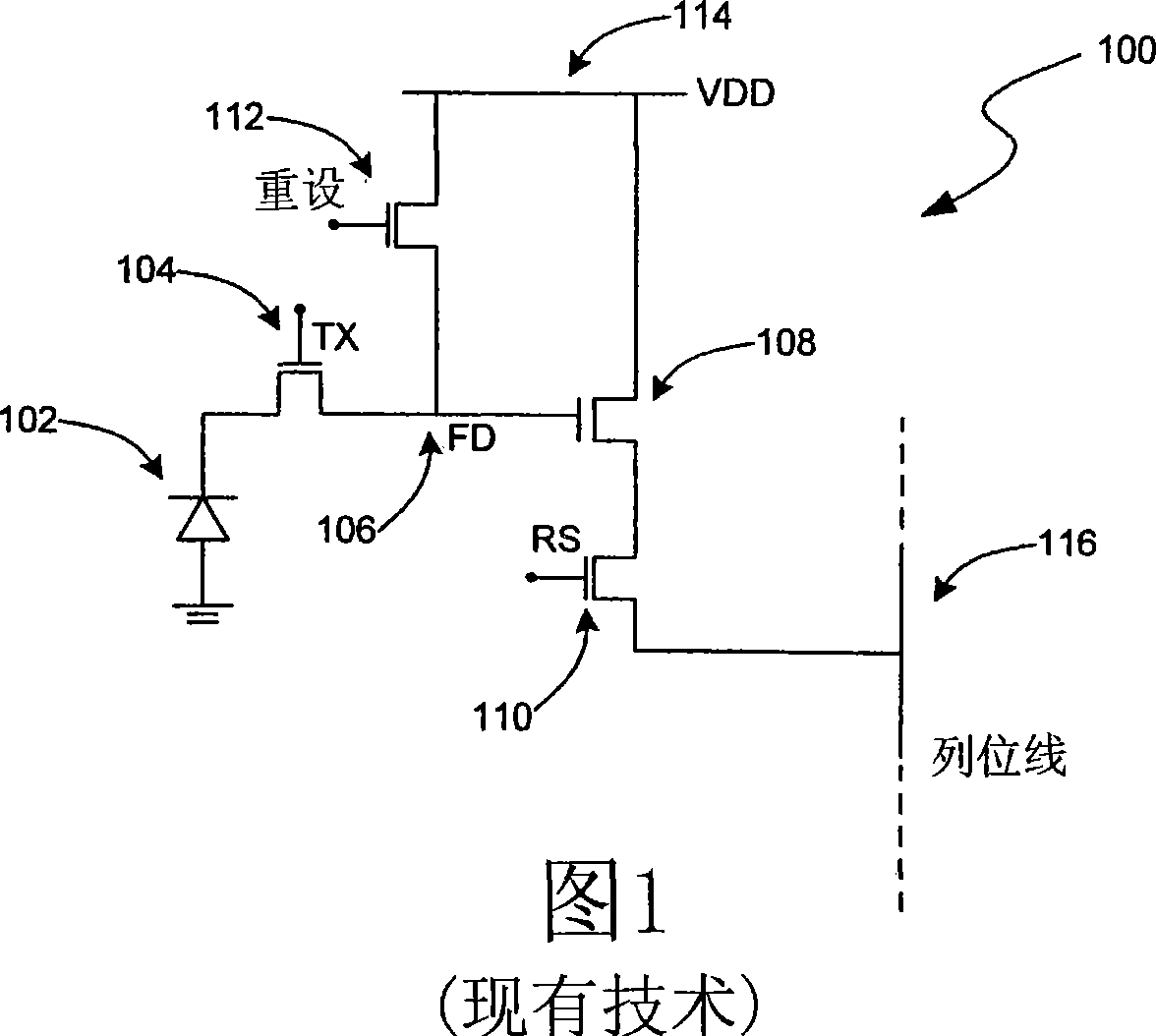
technical field [0001] The present disclosure relates to image sensors with readout noise reduction mechanisms. In particular, aspects of the present disclosure relate to complementary metal oxide silicon (CMOS) image sensors with analog output averaging mechanisms. Background technique [0002] Unlike traditional cameras, which use film to capture and store images, today's digital cameras use solid-state image sensors to acquire images. Such image sensors are typically disposed on a fingernail-sized silicon chip containing millions of optoelectronic devices (eg, photodiodes) arranged in an array of pixels. During exposure, each optoelectronic device records the intensity, or brightness, of incident light by converting light energy into accumulated electrical charges. The brightness recorded by each optoelectronic device can then be read out and stored as a digital signal. [0003] FIG. 1 illustrates a representative solid-state image sensor 100 for acquiring images. Ima...

Claims


Application Information

Patent Timeline
IPC IPC(8): H04N5/217H04N3/15H04N5/357H04N5/378
CPCH04N5/357H04N5/3575H04N5/378H04N25/60H04N25/616H04N25/75
Inventor 阿希什·A·沙阿
Owner OMNIVISION TECH INC
Learn More