Memory device detecting method

A detection method and memory technology, applied in static memory, instruments, etc., can solve problems such as virtual welding, adhesion, and complex address line detection process, and achieve the effect of improving detection efficiency and accurate detection results.

Inactive Publication Date: 2008-06-11
SHENZHEN COSHIP ELECTRONICS CO LTD
1 Cites 24 Cited by

AI-Extracted Technical Summary

Problems solved by technology

[0002] Memory has been widely used in various products in the computer, electronics, and communication industries. Moreover, memory has high requirements for production technology (such as mounting technology). In the case of human factors (such as soldering errors, causing problems such as virtual soldering and adhesion), the memory often has short-circuit or open-circuit problems, which has a great impact on the product and often makes the product unable to operate normally
However, such problems are usually difficult to judge by the naked eye of technicians, and software problems caused by such hardware problems are not easy to locate and difficult to reproduce
[0003] The Chinese patent CN200410069098.2 "Detection method of flash memory" published on January 26, 20...

Abstract

The invention discloses a test method for a storage, which mainly includes three test stages which are respectively read-write test, data wire test and address wire test and search for errors existed in the storage through step-by-step exclusive method which makes test results more accurately. Besides, the invention only needs utilizing the initial address and the final address to comprehensively detect whether the data wire has problems; and for detecting the address wire, the comprehensive test can be performed only by utilizing very few address locations. Moreover, through special arrangement of test data, test data groups and test address blocks, specific data wire and address wire on which an error is existed can be pointed out and the error can be reported in time, thereby greatly improving detection efficiency.

Application Domain

Technology Topic

Image

  • Memory device detecting method
  • Memory device detecting method
  • Memory device detecting method

Examples

  • Experimental program(2)

Example Embodiment

[0075] Example 1
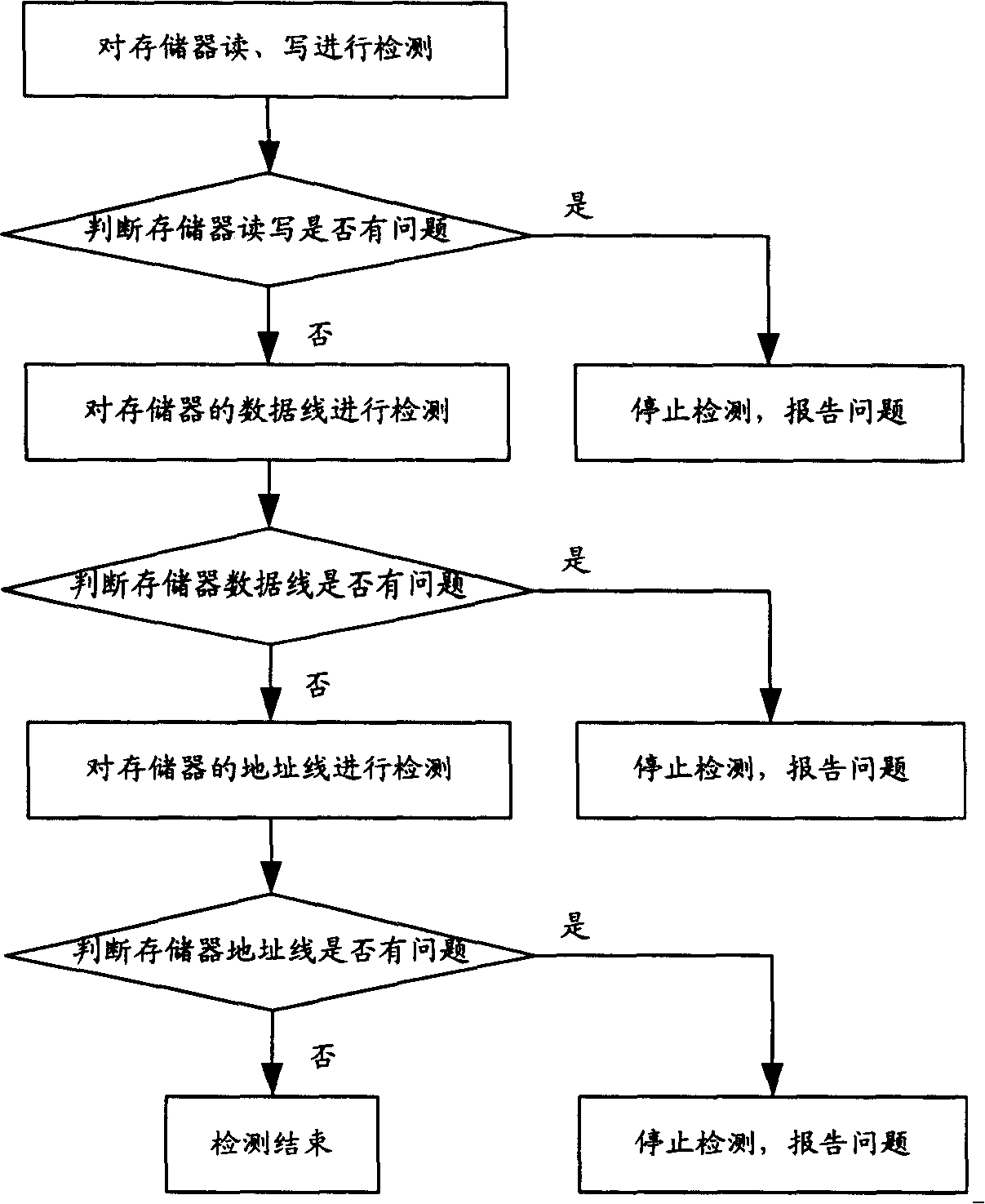
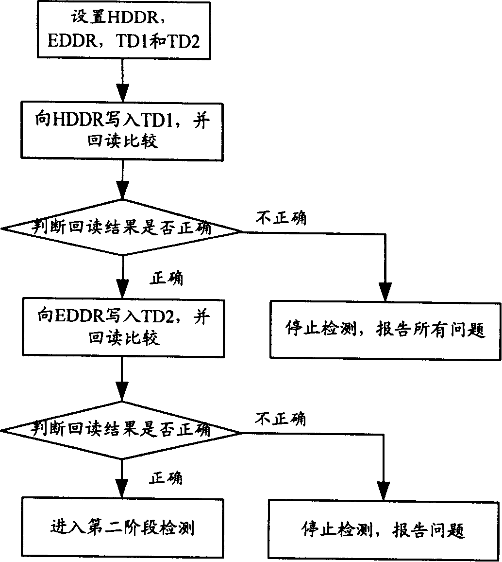
[0076] The first stage, reading and writing testing:
[0077] 1. HDDR is 0X0000000. Because the odd address of the memory cannot be read or written, EDDR is 0X1FFFFFE; for easy detection and calculation, set TD1 to "all 0", that is, 0X0000, and TD2 to "all 1", that is, 0XFFFF.
[0078] TD1 and TD2 can be interchanged, which does not affect the implementation of the present invention. The reason why TD1 and TD2 are set to "all 0" and "all 1" is to facilitate the setting of TDG1 and TDG2 in the second and third stages;
[0079] 2. Write TD1 to HDDR, read back and compare. If the result is correct, it means that each data line is set to low level '0' and it can be normal, which can eliminate the problem of the data line being constantly high level '1', and then , Go to the next step; if the result is not correct, it means that there is a problem in the reading and writing of the HDDR or the address line or the data line, stop the detection and report the problem;
[0080] 3. Write TD2 to EDDR, read back and compare. If the result is correct, it means that each data line is set to high level "1" and it can be normal, which can eliminate the problem of data line being constant low level "0", and then , Enter the second stage of testing; if the result is not correct, it means that there is a problem with EDDR or address line or data line reading and writing, stop testing and report the problem.
[0081] The second stage, data line inspection:
[0082] 1. Suppose the data contained in TDG1 includes: 0X0001, 0X0002, 0X0004, 0X0008, 0X0010, 0X0020, 0X0040, 0X0080, 0X0100, 0X0200, 0X0400, 0X0800, 0X1000, 0X2000, 0X4000, 0X8000;
[0083]2. Write the 16 data of TDG1 into the HDDR in turn, and read back once for each write. If the read back result is correct, continue to write until the 16 data are written and read back, and no problem is found. Then go to step 4;
[0084] 3. If the readback result is incorrect, based on the readback data, it can be judged that there is a problem with the data line corresponding to the "1" bit in the data written to HDDR, record the problem, and then continue to write the remaining data , Until the write-back and read-back are completed, stop the detection and report the found problems;
[0085] For example, after writing all the data in the above TDG1 to HDDR, if the memory is found to have the following two faults, it will report these two faults and stop the detection:
[0086] (1) The written data is 0X0001 and the read data is 0X0000, then the data line D can be judged 0 There is an open circuit fault;
[0087] (2) The written data is 0X0010 and the read data is 0X0000, then the data line D can be judged 4 There is an open circuit fault;
[0088] 4. Suppose the data contained in TDG2 includes: 0XFFFE, 0XFFFD, 0XFFFB, 0XFFF7, 0XFFEF, 0XFFDF, 0XFFBF, 0XFF7F, 0XFEFF, 0XFDFF, 0XFBFF, 0XF7FF, 0XEFFF, 0XDFFF, 0XBFFF, 0X7FFF;
[0089] 5. The 16 data of TDG2 are written into the EDDR in turn. Each time it is written, it is read back once. If the read back result is correct, continue to write until the 16 data are written and read back, and no problem is found. Then enter the third stage of testing;
[0090] 6. If the readback result is incorrect, based on the data read back, it can be judged that there is a problem with the data line corresponding to the "0" bit in the data written to EDDR, record the problem, and then continue to write the remaining data , Until the writing is completed, stop testing and report the problems found;
[0091] For example, after writing all the data in the above TDG2 to EDDR, if the memory has the following two faults, it will report these two faults and stop the detection:
[0092] (1) The written data is 0XFFFE and the read data is 0XFFFF, then the data line D can be judged 0 There is a short-circuit fault;
[0093] (2) The written data is 0XFFEF and the read data is 0XFFFF, then the data line D can be judged 4 There is a short-circuit fault;
[0094] 7. If TDG1 and TDG2 have been written into HDDR and EDDR respectively, and no problems are found, then enter the third stage of testing.
[0095] The third stage, address line detection:
[0096] 1. Write TD1 to HDDR, that is, write data 0X0000 to 0X0000000;
[0097] 2. Because it is a 16-bit data width, the test address must be an even address, so set the test address group 1 to 0X0000002, 0X0000004, 0X0000008, 0X0000010, 0X0000020, 0X0000040, 0X0000080, 0X0000100, 0X0000200, 0X0000400, 0X0000800, 0X0001000, 0X0002000, 0X0004000, 0X0008000, 0X0010000, 0X0020000, 0X0040000, 0X0080000, 0X0100000, 0X0200000, 0X0400000, 0X0800000, 0X1000000, the combination of 24 address units;
[0098] Write TDG1 to the above test address group 1 in sequence. After the 16 data in TDG1 is written to test address group 1, and there are remaining addresses in test address group 1 that have not been tested, continue to write sequentially from the first data of TDG1 Enter, as follows:
[0099] TDG1: Test address group 1:
[0100] 0X0001------------------------0X0000002
[0101] 0X0002------------------------0X0000004
[0102] 0X0004------------------------0X0000008
[0103]...
[0104] 0X0020------------------------0X0400000
[0105] 0X0040------------------------0X0800000
[0106] 0X0080------------------------0X1000000
[0107] After each write, read back the data in 0X0000000. If the read back result is 0X0000, continue to write the next data to the next address until all addresses in the test address group 1 are written and read, and no problem is found , Then go to step 4;
[0108] 3. If the readback result is not 0X0000, it means that the address line with different bits compared with HDDR has a fault. Record the fault and continue writing until all addresses in the test address group 1 have been written and read. , Stop testing and report errors;
[0109] such as:
[0110] (1) After writing 0X0002 to 0X0000002, read back the data in 0X0000000, the read back result is 0X0002, indicating the address line A 1 There is an open circuit problem, and the content originally written to the 0X0000002 address is written to the 0X0000000 address;
[0111] (2) After writing 0X0010 to 0X0000010, read back the data in 0X0000000, the read back result is 0X0010, indicating the address line A 4 There is an open circuit problem, and the content originally written to the address 0X0000010 is written to the address 0X0000000;
[0112] 4. Write TD2 into EDDR, that is, write 0XFFFF into 0X1FFFFFE;
[0113] 5, address group 2 to set the test 0X1FFFFFC, 0X1FFFFFA, 0X1FFFFF6,0X1FFFFEE, 0X1FFFFDE, 0X1FFFFBE, 0X1FFFF7E, 0X1FFFEFE, 0X1FFFDFE, 0X1FFFBFE, 0X1FFF7FE, 0X1FFEFFE, 0X1FFDFFE, 0X1FFBFFE, 0X1FF7FFE, 0X1FEFFFE, 0X1FDFFFE, 0X1FBFFFE, 0X1F7FFFE, 00X1EFFFFE, 0X1DFFFFE, 0X1BFFFFE, 0X17FFFFE, 0X0FFFFFE, the combination of 24 address units;
[0114] Write TDG2 to the above test address group 2 in sequence. After the 16 data in TDG1 have been written to test address group 2, and there are remaining addresses in test address group 2 that have not been tested, continue to write sequentially from the first data of TDG1 Enter, as follows:
[0115] TDG2: Test address group 2:
[0116] 0XFFFE------------------------0X1FFFFFC
[0117] 0XFFFD------------------------0X1FFFFFA
[0118] 0XFFFB------------------------0X1FFFFF6
[0119] 0XFFF7------------------------0X1FFFFEE
[0120] 0XFFEE------------------------0X1DFFFEE
[0121] 0XFFDE------------------------0X1BFFFEE
[0122] 0XFFBE------------------------0X17FFFEE
[0123] 0XFF7E------------------------0X0FFFFEE
[0124] After each write, read back the data in 0X1FFFFFE. If the read back result is 0XFFFF, continue to write the next data to the next address until all addresses in the test address group 2 have been written and read. If not found If there is a problem, it can be judged that the memory read and write, data line and address line are not faulty;
[0125] 6. If the readback result is not 0XFFFF, it means that the address line with different bits compared to EDDR has a fault. Record the fault and continue writing until all addresses in the test address group 2 are written, stop Detect and report errors;
[0126] such as:
[0127] (1) After writing 0XFFFE to 0X1FFFFFC, read back the data in 0X1FFFFFE, the read back result is 0XFFFE, indicating the address line A 1 There is a short circuit problem, and the content originally written to the address 0X1FFFFFC is written to the address 0X1FFFFFE;
[0128] (2) After writing 0XFFF7 to 0X1FFFFEE, read back the data in 0X1FFFFFE, the read back result is 0XFFF7, indicating the address line A 4 There is a short circuit problem, and the content originally written to the 0X1FFFFEE address is written to the 0X1FFFFFE address;
[0129] Through the above-mentioned three-stage detection, the memory read and write problems, data line and address line problems can be detected accurately and comprehensively, and the detection steps are simple and convenient, and a large number of read and write operations are not required, which greatly improves the detection speed.
[0130] Due to different types of memory and different peripheral circuit designs, the same result will indicate different problems. For example, in step 3 of the second stage, the same readback result may be D for some types of memory. 0 And D 4There is a short-circuit fault, so in practical applications, professionals are required to make correct judgments based on the specific hardware schematics.

Example Embodiment

[0131] Example 2
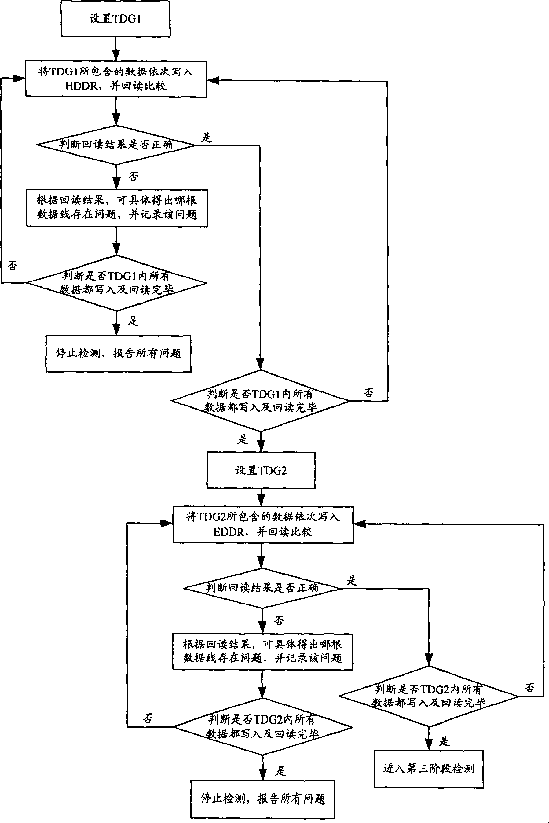
[0132] The difference between this embodiment and embodiment 1 is: in the second and third stages of embodiment 1, if a data line or address line is found to be faulty, the fault is recorded and the detection is continued. In this embodiment, in the second stage and the third stage, as soon as the data line or the address line is found to be faulty, the detection is stopped, the problem is reported, and after the fault is eliminated, the memory detection is restarted. The detection procedures of the second stage and the third stage of this embodiment are as follows: Figure 5 with Figure 6 Shown.

PUM

no PUM

Description & Claims & Application Information

We can also present the details of the Description, Claims and Application information to help users get a comprehensive understanding of the technical details of the patent, such as background art, summary of invention, brief description of drawings, description of embodiments, and other original content. On the other hand, users can also determine the specific scope of protection of the technology through the list of claims; as well as understand the changes in the life cycle of the technology with the presentation of the patent timeline. Login to view more.

Similar technology patents

Classification and recommendation of technical efficacy words

  • Improve detection efficiency
  • The test result is accurate

Materials real-time detection and foreign body eliminating system based on machine vision

InactiveCN101176872AImprove detection efficiencyImprove image quality and accuracy of material detection and foreign object recognitionCharacter and pattern recognitionSortingLight sourceImage identification
Owner:SOUTH CHINA UNIV OF TECH

Non-contact tension detection and feedback control mesh belt winding device

InactiveCN101603244AThe test result is accurateFaster and more effective tension adjustmentAuxillary apparatusMechanical energy handlingImage sensorImage acquisition
Owner:珠海蓝坊智能设备有限公司
Why Eureka
Try Eureka