Method for preventing chip back metal peeling

A backside metal and chip technology, applied in electrical components, semiconductor/solid-state device manufacturing, circuits, etc., can solve problems such as silicon wafer deformation, metal film peeling, peeling, etc., to solve the problem of metal peeling on the back of the chip and reduce mechanical stress Effect

Active Publication Date: 2010-05-19
GTA SEMICON CO LTD
View PDF3 Cites 0 Cited by
  • Summary
  • Abstract
  • Description
  • Claims
  • Application Information

AI Technical Summary

Problems solved by technology

Generally speaking, in order to increase the contact area between the metal layer and the silicon substrate, it is often used to increase the roughness on the back of the silicon wafer. The greater the roughness, the larger the contact area between the metal layer and the silicon substrate, but at the same time Mechanical damage and stress will also increase significantly, resulting in increased fragmentation rates and wafer deformation
At the same time, due to the presence of a large amount of silicon shavings and damaged layers on the surface of the silicon wafer after grinding, the adhesion between the deposited metal film and the substrate decreases and peeling occurs. At the same time, due to the existence of stress, it is possible to Spalling occurs between metal films (usually Ti / Si or Ni / Ag) over time

Method used

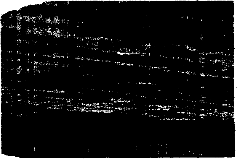
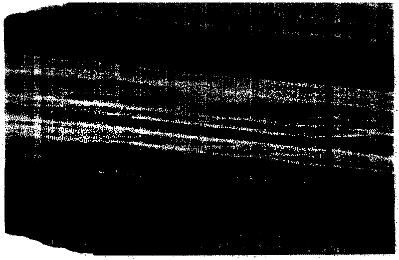
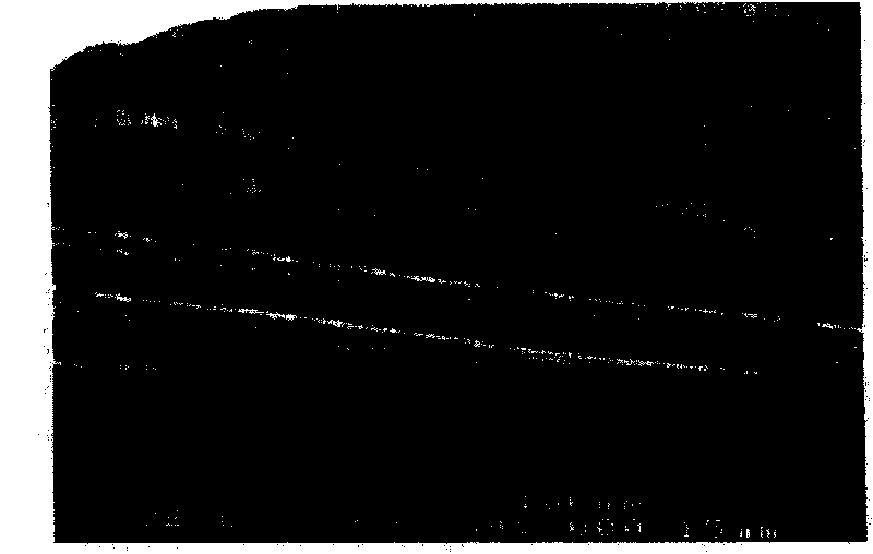

Image

  • Method for preventing chip back metal peeling
  • Method for preventing chip back metal peeling
  • Method for preventing chip back metal peeling

Examples


Embodiment Construction

[0022] The purpose of the present invention is in order to improve the bonding force between the metal on the back side and the deposition substrate silicon, reduce gold-semi-contact resistance simultaneously, seek suitable silicon wafer surface roughness, reduce as far as possible the mechanical stress and the mechanical stress caused by the grinding wafer damage, find an appropriate silicon etching process, and optimize the back gold evaporation process parameters.

[0023] The root of the improvement of the adhesion is to increase the contact area between the metal film and the substrate, so in theory, a backside thinning process with a relatively rough grinding number should be used as much as possible. But in fact, the coarser the grinding number, the more mechanical damage and gravitational force will increase linearly, resulting in an increase in the inline chip loss rate, and at the same time, it will also cause chip cracks and other negative problems during subsequent ...


PUM


Abstract

The invention discloses a method for preventing the metal on the back of a chip from being stripped, which comprises the steps that: the thinning process is applied to the back of the chip adopting apredetermined number of microsections and the damaged silicon layer on the back of the chip is removed using the chemical corrosion solution; the chip is washed using the water so as to remove the residual sully. The method disclosed by the invention can prevent the metal on the back of the chip from being stripped, and can be used for accurately deciding whether the phenomenon of metal strippingexists. The use of the corrosion method effectively removes the damaged silicon layer so as to reduce the mechanical stress. The adoption of the method of controlling the process temperature in the process of evaporization reduces the stress mismatch of the Ti, Ni and Ag three different metals so as to realize solving the problem of the metal stripping on the back of the chip without causing the organic sully.

Description

technical field [0001] The invention relates to a method for metallizing the back of a chip in a semiconductor manufacturing process, more specifically, a method for preventing metal peeling off on the back of a chip in a semiconductor manufacturing process. Background technique [0002] There are many methods for backside metallization of chips. Magnetron sputtering and electron beam evaporation are the most commonly used methods for backside metallization, and their processes have been widely used. Deposition by magnetron sputtering has a high degree of automation, but the throughput is relatively low, and it is an ideal process method below 0.6 μm. In contrast, the method of electron beam evaporation has the following advantages: [0003] 1) The deposited film has high purity and less sodium ion pollution; [0004] 2) Since the evaporation source is only vaporized near the center of the surface, there is no contamination of the crucible; [0005] 3) The integration pro...

Claims


Application Information

Patent Timeline
Patent Type & Authority Patents(China)
IPC IPC(8): H01L21/30H01L21/304H01L21/306H01L21/66
Inventor 金剑华
Owner GTA SEMICON CO LTD
Why Eureka
Try Eureka