LCD device, photoelectric device and process for production thereof

A liquid crystal display device and liquid crystal display panel technology, applied in light guides, optics, optical components, etc., can solve the problems of flexible substrates that are easily deformed, affect the display quality of the display, and cannot fully support the display medium, and achieve the effect of cost increase

Active Publication Date: 2008-07-09
AU OPTRONICS CORP
View PDF0 Cites 41 Cited by
  • Summary
  • Abstract
  • Description
  • Claims
  • Application Information

AI Technical Summary

Problems solved by technology

However, because the flexible substrate is easily deformed, it cannot fully support the display medium...

Method used


Image

  • LCD device, photoelectric device and process for production thereof
  • LCD device, photoelectric device and process for production thereof
  • LCD device, photoelectric device and process for production thereof

Examples


no. 1 example

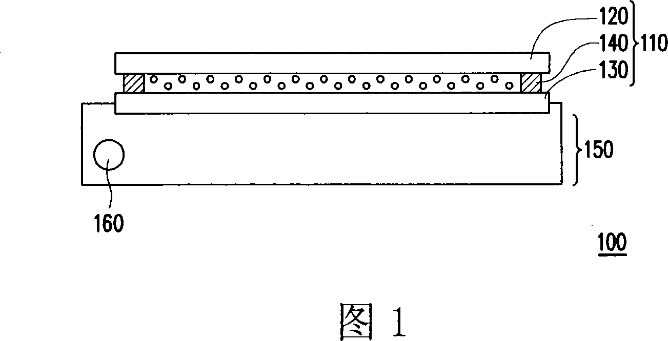
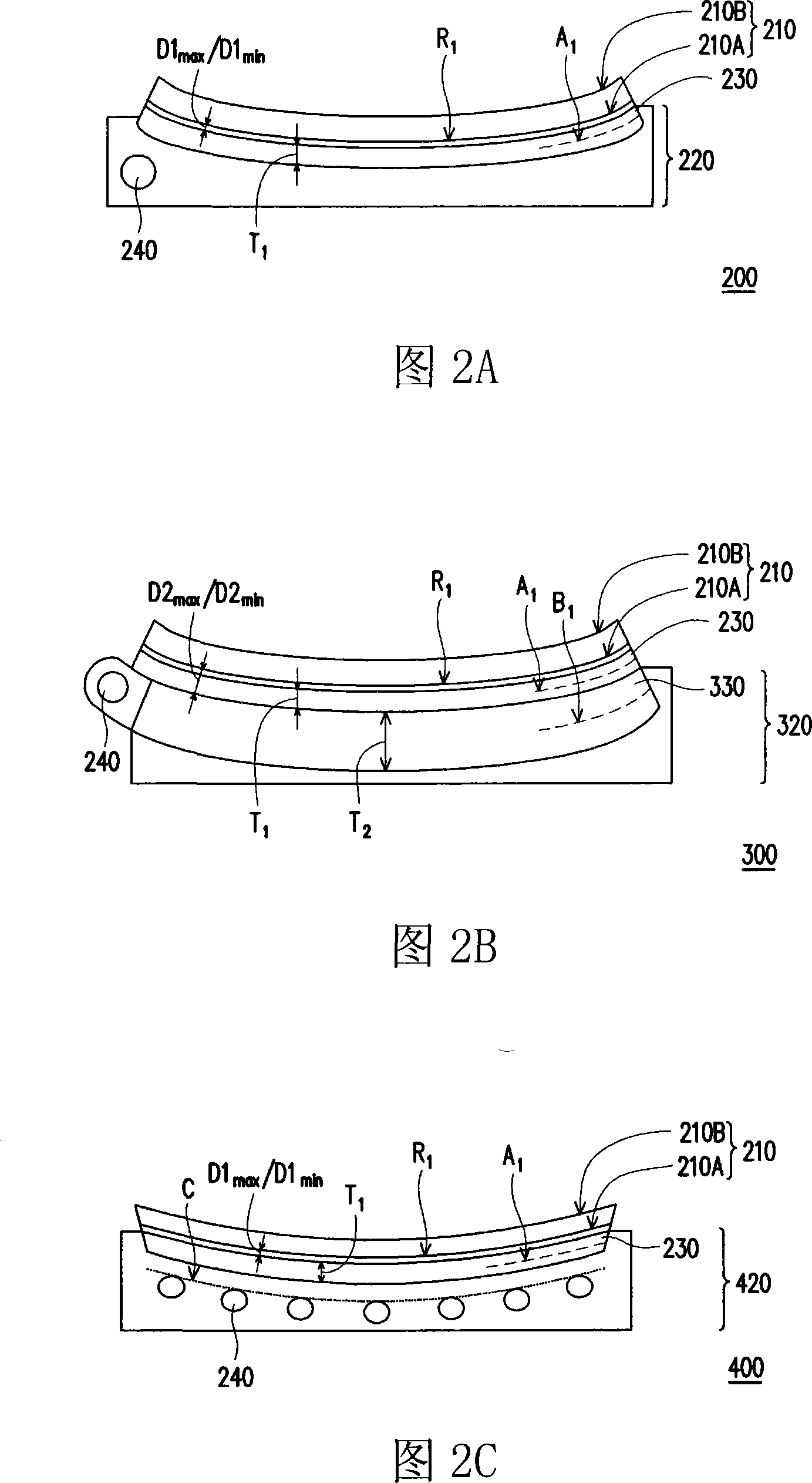
[0061] FIG. 2A is a schematic diagram of a liquid crystal display device of the present invention. Please refer to FIG. 2A , the liquid crystal display device 200 includes a curved liquid crystal display panel 210 and a backlight module 220 . The curved LCD panel 210 has an inner curved surface 210A and an outer curved surface 210B. As shown in FIG. 2A , the outer curved surface 210B is concave. The backlight module 220 is disposed on the inner curved surface 210A of the curved liquid crystal display panel 210, and the backlight module 220 has a curved optical film 230 and a light source 240, wherein the bending degree of the curved optical film 230 and the curved liquid crystal display panel 210 are substantially the same, here It should be noted that when the shortest distance from any point on the curved optical film 230 to the curved liquid crystal display panel 210 is substantially the same, it is defined as the same degree of curvature. In addition, the curved optical ...

no. 2 example

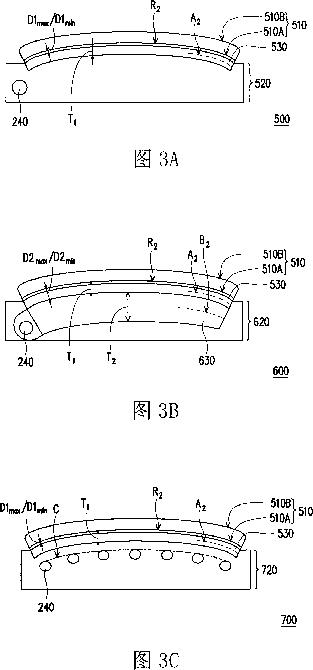
[0070] FIG. 3A is a schematic diagram of a liquid crystal display device of the present invention. Referring to FIG. 3A , the liquid crystal display device 500 includes a curved liquid crystal display panel 510 and a backlight module 520 . The curved LCD panel 510 has an inner curved surface 510A and an outer curved surface 510B. As shown in FIG. 3A , the outer curved surface 510B is convex. The backlight module 520 is disposed on the inner curved surface 510A of the curved liquid crystal display panel 510, and the backlight module 520 has a curved optical film 530 and a light source 240, wherein the bending degree of the curved optical film 530 and the curved liquid crystal display panel 510 are substantially the same, here It should be noted that when the shortest distance from any point on the curved optical film 530 to the curved liquid crystal display panel 510 is substantially the same, it is defined as the same degree of curvature.

[0071] Specifically, the thickness...


PUM


Abstract

The invention relates to an LCD device, a photoelectric device and a manufacture method thereof. The LCD device comprises a bending LCD panel and a backlight module, wherein the bending LCD panel includes an inner curved surface and an outer curved surface; the backlight module is arranged on the inner curved surface of the bending LCD panel and includes a bending optical film and a light source; and the bending degree of the bending optical film is substantially equal to that of the bending liquid display panel. Accordingly, the LCD device has flexibility. The LCD device of the invention is mainly composed of the bending LCD panel and the backlight module having the bending optical film, and the bending degree of the bending optical film is substantially equal to that of the bending LCD panel. Accordingly, the LCD device has flexibility to meet the more use requirement. Additionally, the fabrication method of the LCD device is compatible to prior art and technique, thus obviating the addition of extra equipment and the increase of cost.

Description

technical field [0001] The present invention relates to a display device, and in particular to a bendable display device. Background technique [0002] The rapid progress of the multimedia society is mostly due to the rapid progress of semiconductor components or man-machine display devices. As far as display devices are concerned, flat panel display devices with superior characteristics such as high image quality, good space utilization efficiency, low power consumption, and no radiation have gradually become the mainstream of the market. Among various flat-panel display devices, a liquid crystal display (Liquid Crystal Display, LCD) is currently the most mature flat-panel display device. [0003] FIG. 1 is a schematic diagram of a prior art liquid crystal display device. Please refer to FIG. 1, the liquid crystal display device 100 includes a liquid crystal display panel 110 and a backlight module 150, wherein the liquid crystal display panel 110 includes a color filter ...

Claims


Application Information

Patent Timeline
IPC IPC(8): G02F1/13357G02B6/00G02F1/1333G02F1/1335
Inventor 储中文刘昱辰林朝成吴哲耀陈群元
Owner AU OPTRONICS CORP
Why Eureka
Try Eureka