

Touch screen device and debugging method thereof
A debugging method and touch screen technology, applied in the input/output process of data processing, instruments, electrical digital data processing and other directions, can solve problems such as inconvenience, low light energy, touch screen coordinate detection interference, etc., to achieve convenient debugging and cost saving Effect
- Summary
- Abstract
- Description
- Claims
- Application Information
AI Technical Summary
Problems solved by technology
Method used
Image

Examples
Embodiment 1
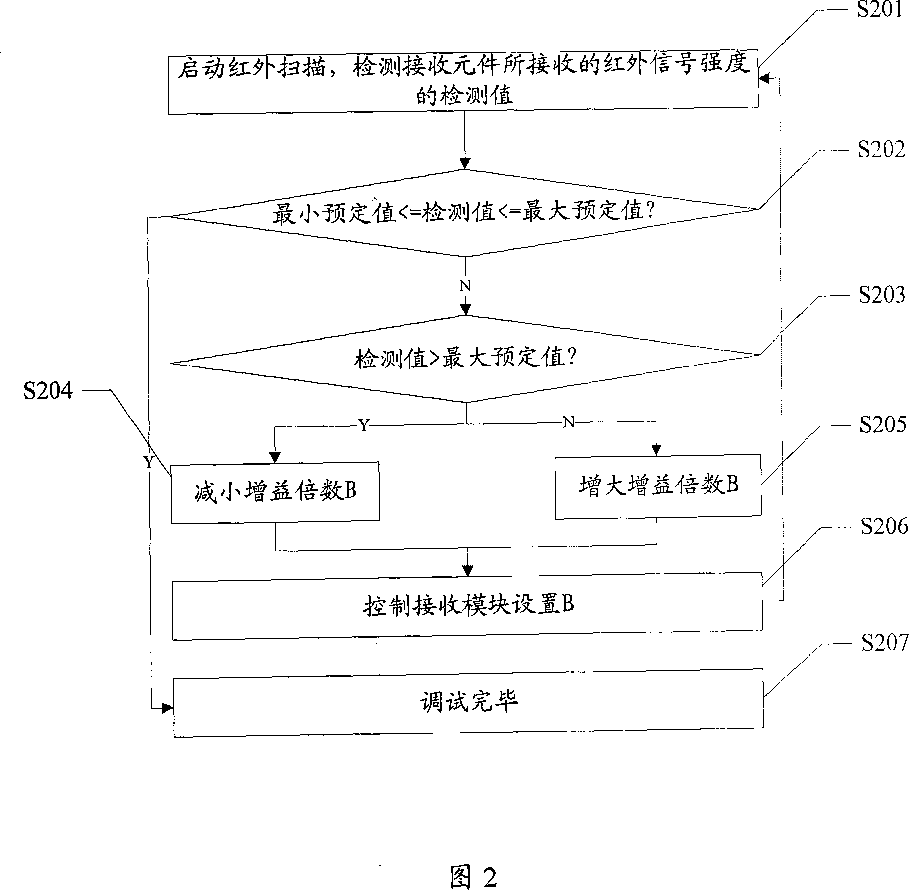
[0026] As shown in FIG. 2, it is a schematic flowchart of Embodiment 1 of the debugging method of the touch screen device of the present invention. In this embodiment, when debugging, only the gain multiple of the receiving circuit corresponding to the receiving element is modified.
[0027] As shown in the figure, it includes the steps:
[0028] Step S201: Start an infrared scan to detect the intensity value of the infrared signal received by the infrared receiving element, which is called the detection value, and go to step S202;
[0029] Step S202: Determine whether the detection value is greater than or equal to the minimum predetermined value and less than or equal to the maximum predetermined value, that is, whether the minimum predetermined value <= the detection value <= the maximum predetermined value is satisfied, if not, go to step S203, if yes, Then there is no need to debug or complete the debugging of the relevant device parameters corresponding to the current infrar...
Embodiment 2
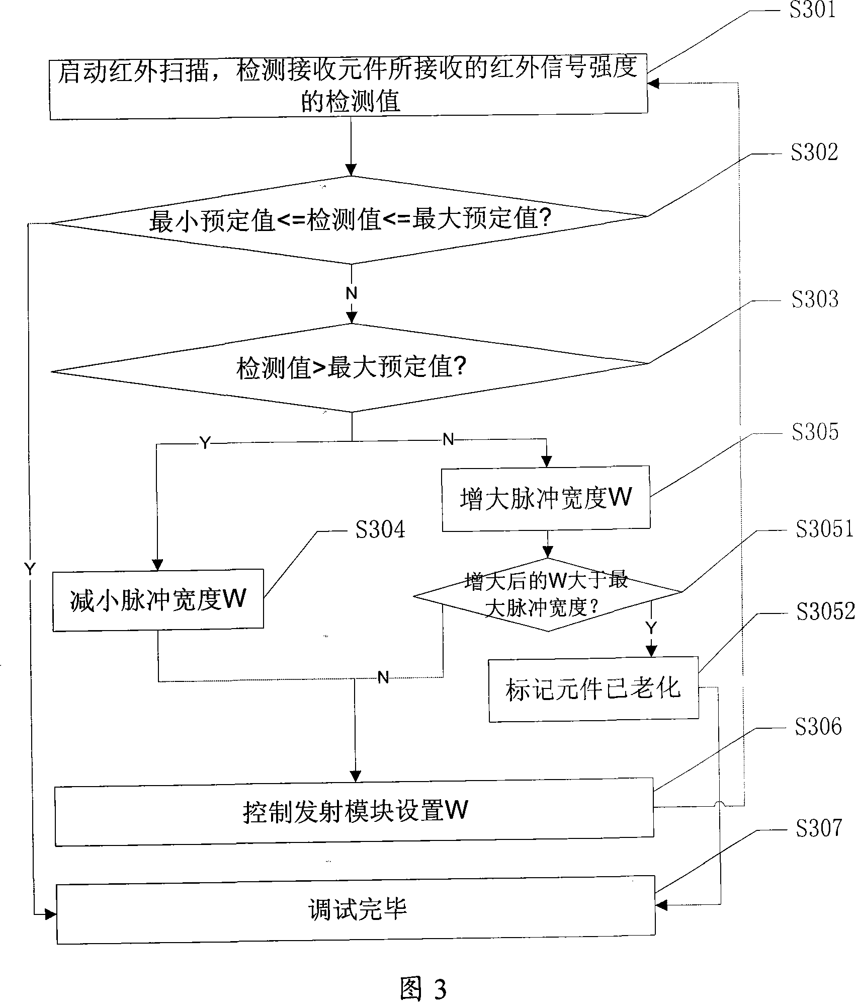
[0045] As shown in FIG. 3, it is a schematic flowchart of the second embodiment of the debugging method of the touch screen device of the present invention. In this embodiment, when debugging, only the pulse width of the transmitting circuit corresponding to the transmitting element is adjusted.
[0046] As shown in the figure, it includes the steps:
[0047] Step S301: Start an infrared scan to detect the intensity value of the infrared signal received by the infrared receiving element, which is called the detection value, and go to step S302;
[0048] Step S302: Determine whether the detection value is greater than or equal to the minimum predetermined value and less than or equal to the maximum predetermined value, that is, whether the minimum predetermined value <= the detection value <= the maximum predetermined value is satisfied, if not, go to step S303, if yes, Then there is no need to debug or complete the debugging of the relevant device parameters corresponding to the c...
Embodiment 3
[0066] There are many reasons why the signal strength received by the infrared receiving element is outside the optimal range. For example, the aging of the transmitting element causes the intensity of the infrared signal emitted under the same pulse width to become lower, and the aging of the receiving element causes the receiving sensitivity to decrease, As well as some other external factors such as dust occlusion, etc., therefore, in this embodiment, the pulse width of the transmitting circuit corresponding to the infrared emitting element and the gain multiple of the receiving circuit corresponding to the infrared receiving element are adjusted simultaneously. Elaboration.
[0067] As shown in the figure, in this embodiment, it includes the steps:
[0068] Step S401: Start an infrared scan to detect the intensity value of the infrared signal received by the infrared receiving element, which is called the detection value, and go to step S402;
[0069] Step S402: Determine whet...
PUM
 Abstract
Description
Claims
Application Information