Scheduling method of silicon slice transmission course

A technology of transmission process and scheduling method, applied in the direction of conveyor objects, transportation and packaging, electrical program control, etc., can solve the problems of long manufacturing cycle and low production efficiency, and achieve short manufacturing cycle, high production efficiency, and silicon wafer transmission reasonable effect

Active Publication Date: 2008-07-23
BEIJING NAURA MICROELECTRONICS EQUIP CO LTD
View PDF0 Cites 11 Cited by
  • Summary
  • Abstract
  • Description
  • Claims
  • Application Information

AI Technical Summary

Problems solved by technology

In this way, most of the nodes are idle, and the path of silicon chip transmission is not necessarily the shortest path. The manufacturing cycle is longer and the production efficiency is low.

Method used


Image

  • Scheduling method of silicon slice transmission course

Examples


Embodiment Construction

[0034] The scheduling method of the silicon chip transmission process of the present invention is mainly used in the semiconductor silicon chip processing process to schedule the transmission paths of a plurality of silicon chips in N nodes in the silicon chip processing equipment, wherein N is a positive integer, and can also be used For the scheduling of other transmission equipment.

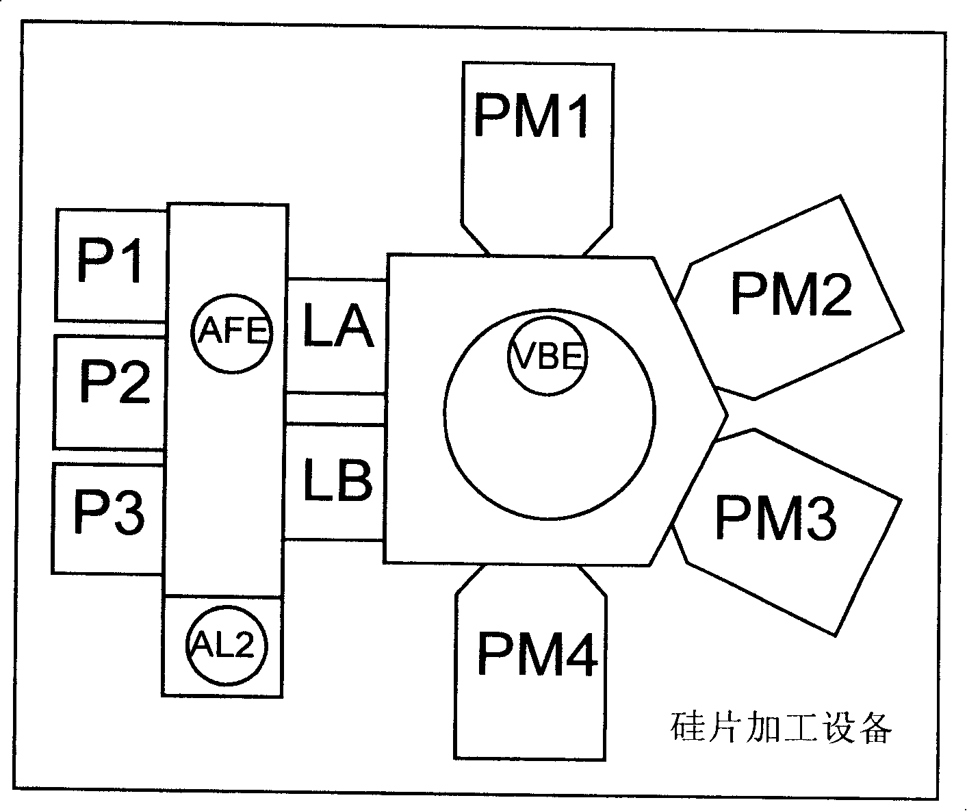
[0035] Such as figure 1 As shown, the silicon wafer processing equipment includes the following nodes:

[0036] The first film chamber P1; the second film chamber P2; the third film chamber P3; the positioning calibration device AL2; the first vacuum lock LA; the second vacuum lock LB; the atmospheric manipulator AFE; the vacuum manipulator VBE; the first reaction chamber PM1; The second reaction chamber PM2; the third reaction chamber PM3; the fourth reaction chamber PM4.

[0037] The scheduling method of the silicon chip transmission process of the present invention can calculate the short...


PUM


Abstract

The invention discloses a dispatching method in the process of transiting silicon chips, which comprises firstly calculating the transmission cost S(i)(j) of joints from the ith to the jth of any silicon chip in a plurality of silicon chips, then calculating the transmission costs S(i)(k)+S(i)(k) of joints from the ith to the kth and from the kth to the jth of the silicon chip, comparing S(i)(j) with S(i)(k)+S(i)(k), if S(i)(j)>S(i)(k)+S(i)(k), then replacing S(i)(j) with S(i)(k)+S(i)(k), and so forth, finally obtaining the least transmission cost S(i)(j) min of joints from the ith to the jth of the silicon chip, which is the shortest way. The invention has the advantages that the transmission of the silicon chip is reasonable, the manufacturing period is short, the work efficiency is high, and the invention is mainly adapted to the manufacturing procedure of semi-conductor silicon chip and dispatches the transmission of the silicon chips in the silicon chip processing device.

Description

technical field [0001] The invention relates to a production process scheduling method, in particular to a scheduling method for the silicon wafer transmission process in the semiconductor silicon wafer processing technology. Background technique [0002] Processing semiconductor silicon wafers requires multiple processes, and silicon wafer processing equipment includes multiple chambers for processing silicon wafers. Such as figure 1 As shown, it includes four reaction chambers for etching silicon wafers, which are respectively PM1, PM2, PM3, and PM4; it also includes three film chambers, which are respectively P1, P2, and P3, for storing Silicon wafer; also includes an AL2 (positioning and calibration device) for positioning and calibrating the silicon wafer; also includes an atmospheric transmission chamber and a vacuum transmission chamber, which are communicated through LA and LB (vacuum lock). There is an AFE (atmospheric manipulator) in the atmospheric transfer cham...

Claims


Application Information

Patent Timeline
Patent Type & Authority Applications(China)
IPC IPC(8): H01L21/00H01L21/677G05B19/04
Inventor 崔琳
Owner BEIJING NAURA MICROELECTRONICS EQUIP CO LTD
Why Eureka
Try Eureka