High frequency switch circuit
一种高频开关、开关电路的技术,应用在电子开关、电气元件、脉冲技术等方向,能够解决不能够获得信号隔离性能、开关电路独立提供电源、电路的元件数量巨大等问题,达到节省芯片面积、低成本、降低功率消耗的效果
- Summary
- Abstract
- Description
- Claims
- Application Information
AI Technical Summary
Problems solved by technology
Method used
Image

Examples
Embodiment 1
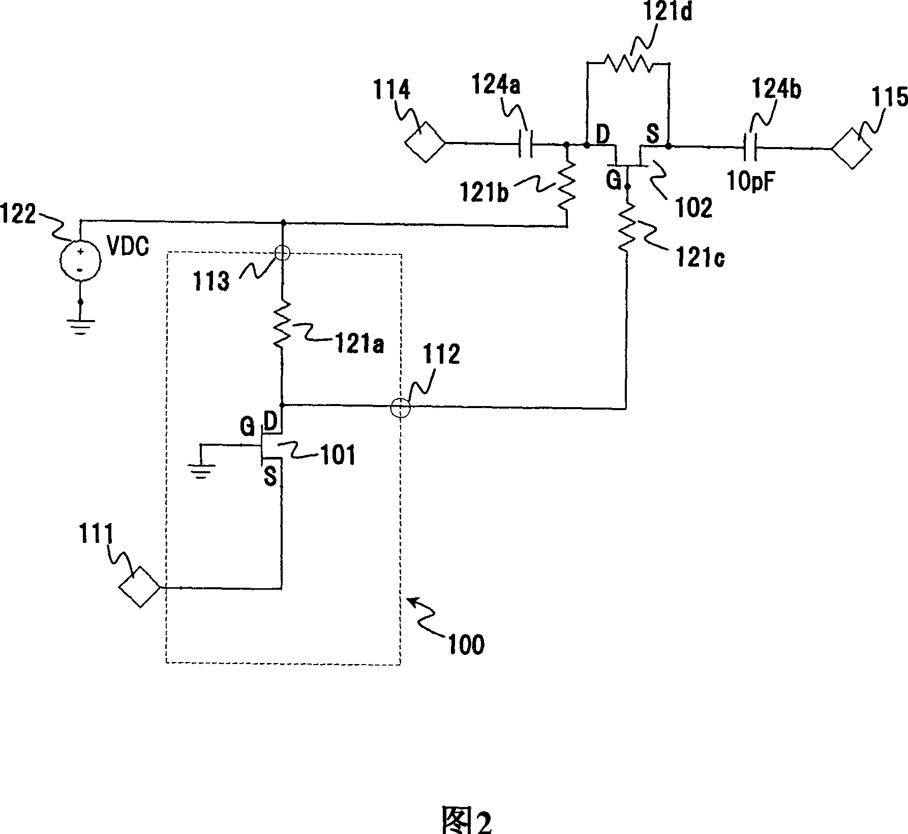
[0052] Fig. 2 is a circuit diagram of a high frequency switching circuit as a first embodiment according to the present invention. In the figure, reference numerals 114 and 115 respectively denote an input terminal 114 and an output terminal 115 of a high-frequency signal in the high-frequency switching circuit. Reference numerals 101 and 102 denote depletion type field effect transistors, and reference numerals 121a to 121d denote resistors. An input terminal 114 and an output terminal 115 of a high-frequency signal are supplied by a switch circuit including a depletion field effect transistor 102 for performing switching between a connected state and a disconnected state of a high-frequency signal path.
[0053] Note that, in the present embodiment, the resistor 121a used in the control voltage generating circuit 100 is a resistor made of a tantalum nitride thin film. Also, reference numerals 124a and 124b denote capacitors serving as sufficiently small impedance in a high ...
Embodiment 2
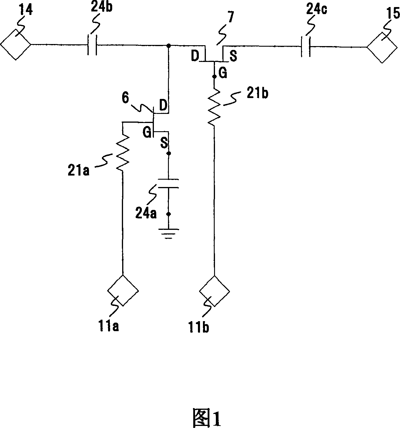
[0067] Fig. 4 is a circuit diagram of a high-frequency switching circuit as a second embodiment of the present invention. Note that in this figure, the same elements as those shown in FIG. 2 are denoted by the same reference numerals and symbols. In this high-frequency switching circuit, the gate of the field effect transistor 101 used in the control voltage generating circuit 100 is grounded through a resistor 121e.
[0068] Since the gate of the field effect transistor 101 is grounded through the resistor 121e in this way, even when an excessively high voltage is input from the external control signal input terminal 111, a current caused by the excessively high voltage must flow through the resistor 121a and the resistor 121e. , thereby suppressing the voltage applied to the field effect transistor 101 (the current flowing through the transistor).
[0069] In this way, the field effect transistor 101 is protected over a certain range with respect to the overvoltage input, a...
Embodiment 3
[0074] FIG. 5 is a circuit diagram of a high-frequency switching circuit as a third embodiment of the present invention. In this embodiment, a single pole double throw (SPDT) circuit is implemented. Note that also in FIG. 5 , the same elements as those shown in FIG. 2 are denoted by the same reference numerals and symbols. However, in conformity therewith, the high-frequency switching circuit is provided with two control voltage generating circuits (100a, 100b), for example, as in the external control signal input terminals 111a and 111b, suffixes a and b are respectively attached to the control voltage generating circuits of multiple components.
[0075] Hereinafter, the operation of the high-frequency switch circuit according to the present embodiment will be described. The high frequency switching circuit according to the present embodiment includes two control voltage generating circuits 100a and 100b, and applies complementary external control voltages from logic circui...
PUM
 Abstract
Description
Claims
Application Information
 - R&D Engineer
- R&D Manager
- IP Professional
- Industry Leading Data Capabilities
- Powerful AI technology
- Patent DNA Extraction
Browse by: Latest US Patents, China's latest patents, Technical Efficacy Thesaurus, Application Domain, Technology Topic.
© 2024 PatSnap. All rights reserved.Legal|Privacy policy|Modern Slavery Act Transparency Statement|Sitemap