

High light transmittance ratio transparent resin display protection panel and LCD device using same
A liquid crystal display, transparent resin technology, applied in shielding, instruments, optics, etc., can solve the problems of easy rainbow, low yield, and difficult to control film thickness.
- Summary
- Abstract
- Description
- Claims
- Application Information
AI Technical Summary
Problems solved by technology
Method used
Image

Examples
Embodiment 1
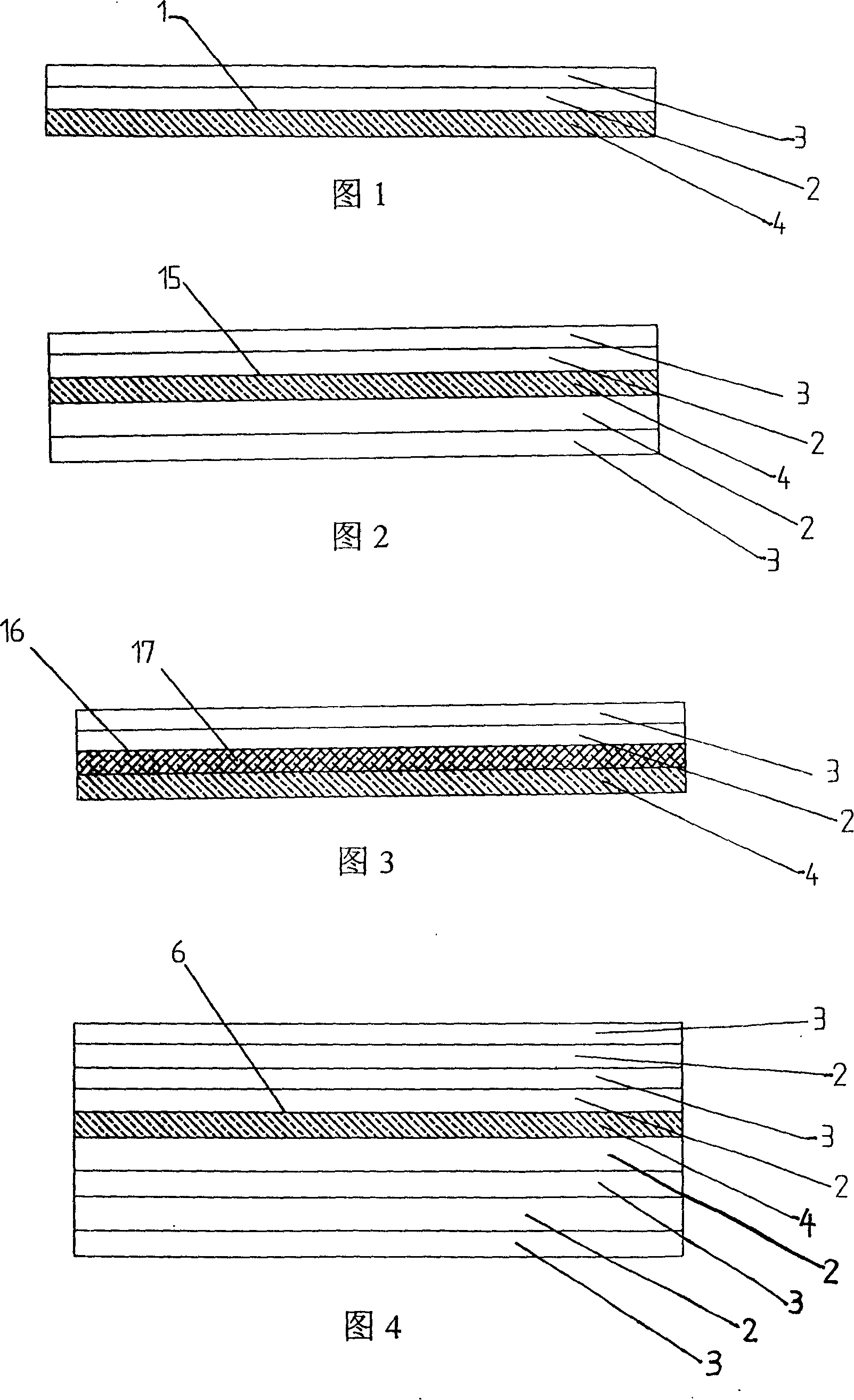
[0031] Fig. 1 has provided present embodiment 1 figure. Referring to Fig. 1, the display protective screen 1 of high light transmittance transparent resin is made of a transparent transparent resin substrate 4 and a two-layer anti-reflection and anti-reflection TiO deposited sequentially by a vacuum magnetron sputtering method on one side of the substrate 4. 2 Coating 2 and SiO 2 The film layer 3 is formed, and the formation structure is SiO 2 / TiO 2 A display protective screen 1 of a transparent resin substrate with high light transmittance.
Embodiment 2
[0033] Fig. 2 has provided present embodiment 2 figure. Referring to Fig. 2, the display protective screen 15 of high light transmittance transparent resin is made of transparent transparent resin substrate 4 and adopts the TiO of two layers of antireflection and antireflection deposited successively by vacuum magnetron sputtering method on both sides of substrate 4 2 Coating 2 and SiO 2 The film layer 3 is formed, and the formation structure is SiO 2 / TiO 2 / Transparent resin substrate / TiO 2 / SiO 2 The display protective screen 15 of high light transmittance transparent resin. Two layers of anti-reflection and anti-reflection coatings are coated on both sides of the substrate 4, the light transmittance is greater than 94%, the double-sided superimposed reflectance is less than 2%, and the optimized thickness of the coating is: TiO 2 10~16nm, SiO 2 It is 90~120nm.
Embodiment 3
[0035] Fig. 3 has provided the figure of present embodiment 3, and present implementation is basically the same as embodiment 1, and difference is that on one side of substrate 4 and the TiO of antireflection and antireflection 2 An acrylic resin layer 17 that increases the hardness and light transmittance of the substrate is coated between the film layers 2, and the structure is SiO 2 / TiO 2 / Acrylic resin layer / Transparent resin substrate The display protective screen 16 of high light transmittance transparent resin. Coating a layer of acrylic resin can not only increase the light transmittance of the substrate by 1 to 2 percentage points, but also provide a surface hardness of more than 2H, so that the surface after coating has a pencil test hardness greater than 2H. At the same time, the formula can be adjusted to make the coating The adhesion between the layer and the substrate is greatly enhanced.
PUM
| Property | Measurement | Unit |
|---|---|---|
| thickness | aaaaa | aaaaa |
| thickness | aaaaa | aaaaa |
| thickness | aaaaa | aaaaa |
Abstract
Description
Claims
Application Information