Contact and electrical connector

A technology of electrical connectors and contacts, which is applied in the direction of contact parts, connection, fixed connection, etc., and can solve problems such as imparting appropriate contact pressure to the non-contact portion 122c, contact pressure, deformation, and lack of bending amount

Inactive Publication Date: 2008-10-08
TYCO ELECTRONICS JAPAN GK
View PDF1 Cites 7 Cited by
  • Summary
  • Abstract
  • Description
  • Claims
  • Application Information

AI Technical Summary

Problems solved by technology

[0013] That is, for some reason, the IC package 130 and the circuit board 140 may be either bent or deformed.
In this case, when the conductive pad provided on the IC package 130 is brought into contact with and pressed to the contact portion 122c, and the conductive pad provided on the circuit board 140 is brought into contact with and pressed to the contact portion 123c, the first elasticity of the contact 120 cannot be obtained. The desired amount of bending of the contact

Method used


Image

  • Contact and electrical connector
  • Contact and electrical connector
  • Contact and electrical connector

Examples


Embodiment Construction

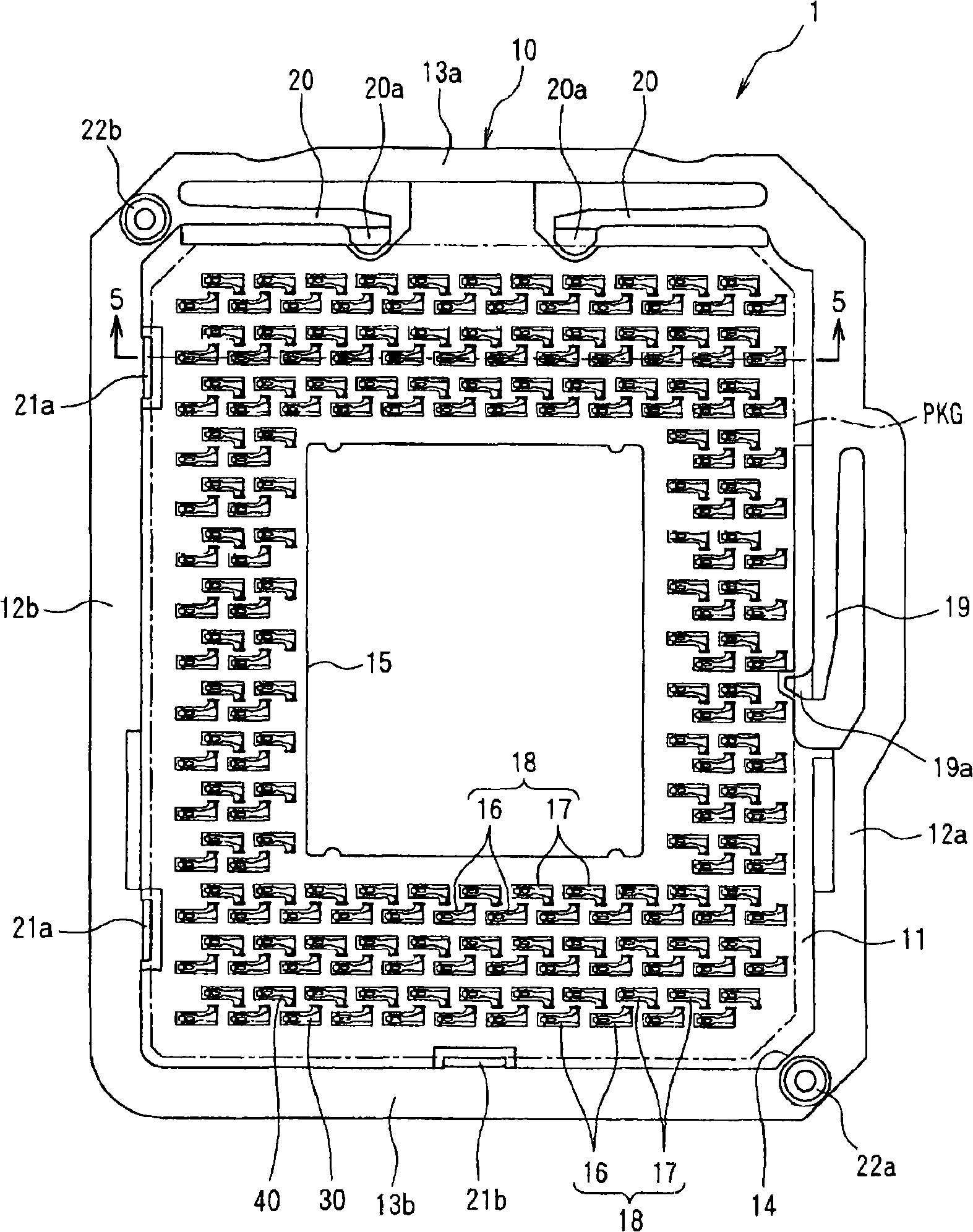
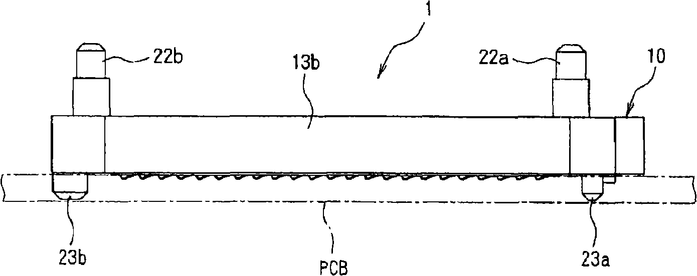
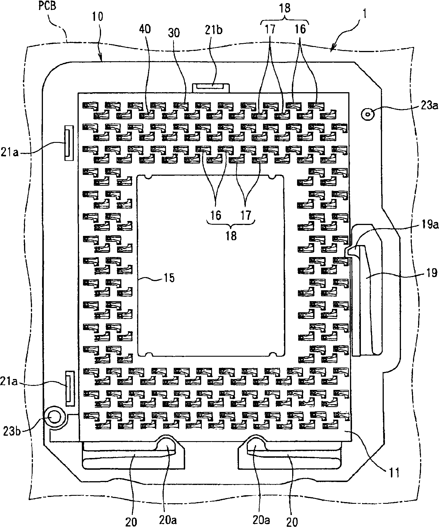
[0072] Hereinafter, embodiments of the present invention will be described with reference to the drawings. figure 1 is a plan view of the electrical connector of the present invention, wherein the IC components are represented together by dotted and dashed lines. figure 2 yes figure 1 front view of the electrical connector, image 3 yes figure 1 The bottom view of the electrical connector, where, in figure 2 and image 3 In , circuit boards are collectively represented by dotted lines. Figure 4 is a representation of figure 1 A partial plan view of the column of contact housing cavities in Figure 5 is along the figure 1 The sectional view of line 5-5 in Figure 6 is a representation of the image 3 A partial bottom view of an example of a contact housing cavity.

[0073] exist Figure 1 ~ Figure 3 Among them, the electrical connector 1 includes: an insulating housing 10 , a plurality of first contacts 30 fixed to the housing 10 , and a plurality of second contac...


PUM


Abstract

Provided are a contact, which improves contact reliability of a contact section of a first elastic contact arm which makes contact with a conductive pad of an IC package and reliability of a contact section of a second elastic contact arm which makes contact with a conductive pad of a circuit board, and an electrical connector. The contacts (30, 40) of the electrical connector (1) are provided with substantially rectangular substrate sections (31, 41), which are fixed in contact storing cavities (16, 17) of a housing (10) and extend in the vertical direction; connecting pieces (32, 42), which extend in a direction orthogonally intersecting main planes of the substrate sections (31, 41) from the substrate sections (31, 41); the first elastic contact arms (34, 44), which extend diagonally upward from leading ends of the connecting pieces (32, 42) and have contact sections (34c, 44c) making contact with the conductive pad of an IC package (PKG); and the second elastic contact arms (35, 45), which diagonally extend downward from leading ends of the connecting pieces (32, 42) and have contact sections (35c, 45c) making contact with the conductive pad of the circuit board (PCB).

Description

technical field [0001] The present invention relates to a contact and an electrical connector for electrically connecting an IC package on which an IC such as a DMD (Digital micromirrodevice: digital micromirror device) is mounted, to a circuit board. Background technique [0002] Conventionally, as an electrical connector for electrically connecting an IC package to a circuit board, for example, known Figure 15 and Figure 16 The device shown (refer to Patent Document 1). Figure 15 is a perspective view showing electrical connectors together with IC components, Figure 16 is along Figure 15 Sectional drawing of line 16-16. [0003] exist Figure 15 and Figure 16 Among them, the electrical connector 101 includes an insulating housing 110 and a plurality of contacts 120 mounted on the housing 110 . [0004] The case 110 includes a substantially rectangular plate-shaped base portion 111 mounted on a circuit board 140 , and a side wall 112 constituted by four sides risin...

Claims


Application Information

Patent Timeline
IPC IPC(8): H01R33/76H01R13/24
CPCH05K7/1069H01R13/2435H01R12/7076H01R13/24H01R12/51
Inventor 桥本信一白井浩史
Owner TYCO ELECTRONICS JAPAN GK
Why Eureka
Try Eureka