Multi-chip encapsulation storage module

A memory module and memory technology, applied in information storage, static memory, digital memory information, etc., can solve problems such as inability to realize function expansion, and achieve the effect of reducing the number of external interface pins

Inactive Publication Date: 2008-11-12
POTEVIO INFORMATION TECH
View PDF0 Cites 8 Cited by
  • Summary
  • Abstract
  • Description
  • Claims
  • Application Information

AI Technical Summary

Problems solved by technology

[0006] However, the existing MCP storage modules are limited

Method used


Image

  • Multi-chip encapsulation storage module
  • Multi-chip encapsulation storage module
  • Multi-chip encapsulation storage module

Examples


Embodiment 1

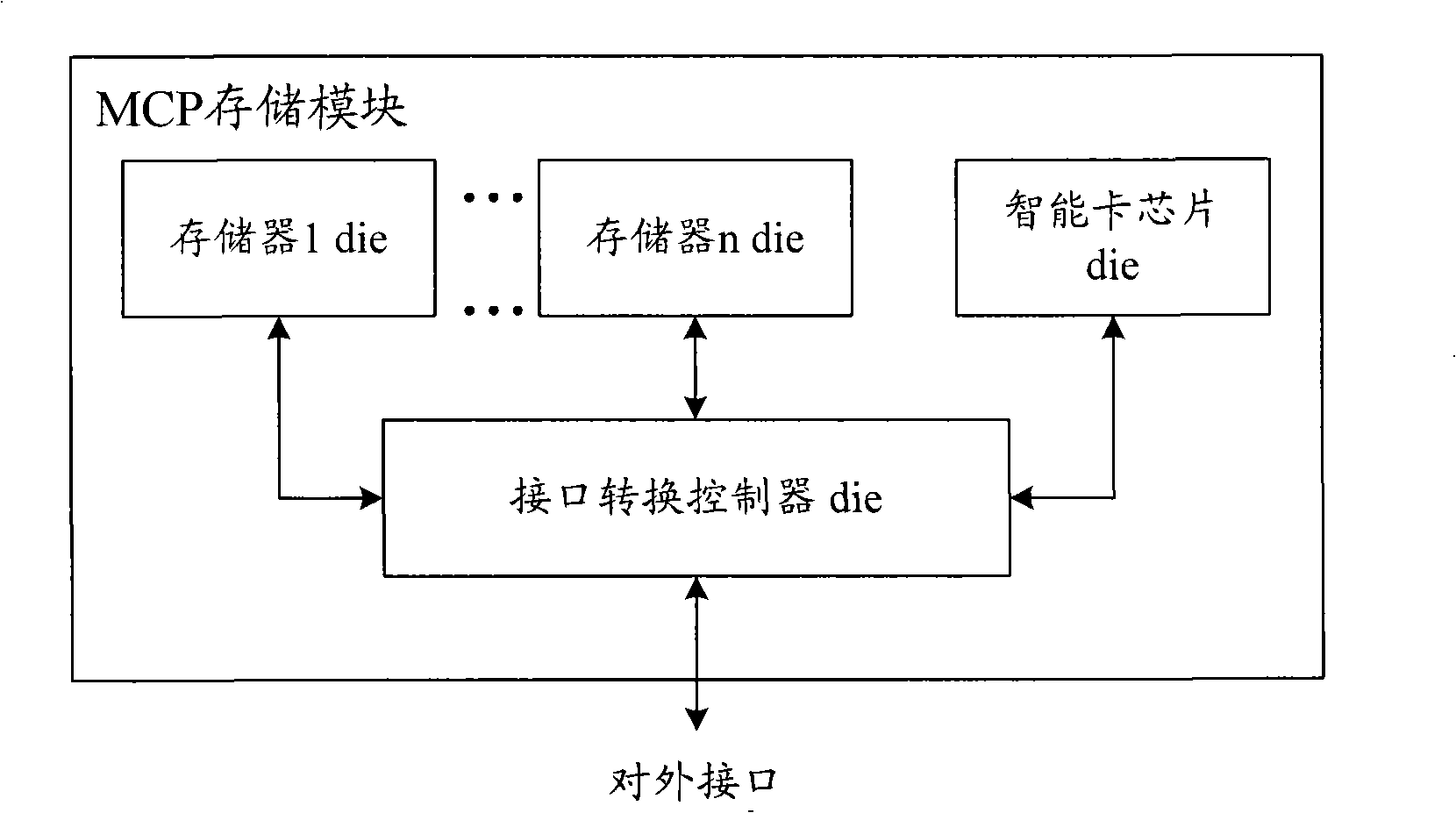
[0050] image 3 It is a schematic structural diagram of the MCP storage module in Embodiment 1 of the present invention. Such as image 3 As shown, taking SDRAM and NAND Flash as examples, in image 3 middle( image 3 The "die" in represents the die), the SDRAM and NAND Flash in the MCP storage module are connected to the interface conversion controller through the SDRAM bus and the NAND Flash bus respectively, and the smart card chip is connected to the interface conversion controller through the smart card chip bus.

[0051] Such as image 3 The MCP storage module shown has three external interfaces corresponding to SDRAM, NAND Flash, and smart card chips one by one, that is, the SDRAM bus external interface corresponding to SDRAM, the NAND Flash bus external interface corresponding to NAND Flash, and the smart card chip. The corresponding smart card chip bus external interface.

[0052] In this way, the interface conversion controller is connected to the external interfa...

Embodiment 2

[0077] Figure 6 It is a schematic structural diagram of the MCP storage module in Embodiment 2 of the present invention. Such as Figure 6 As shown, still taking SDRAM and NAND Flash as examples, in Figure 6 middle( Figure 6 The "die" in represents the die), the SDRAM and NAND Flash in the MCP storage module are connected to the interface conversion controller through the SDRAM bus and the NAND Flash bus respectively, and the smart card chip is connected to the interface conversion controller through the smart card chip bus.

[0078] Such as Figure 6 The MCP storage module shown has only one external interface. Of course, the MCP storage module may also have more than one external interface, but it does not correspond to SDRAM, NAND Flash, and smart card chips one by one. Preferably, since the transmission rate of the SDRAM bus is relatively fast, in order to improve the access efficiency of the external host to the MCP storage module, one external interface in this em...

Embodiment 3

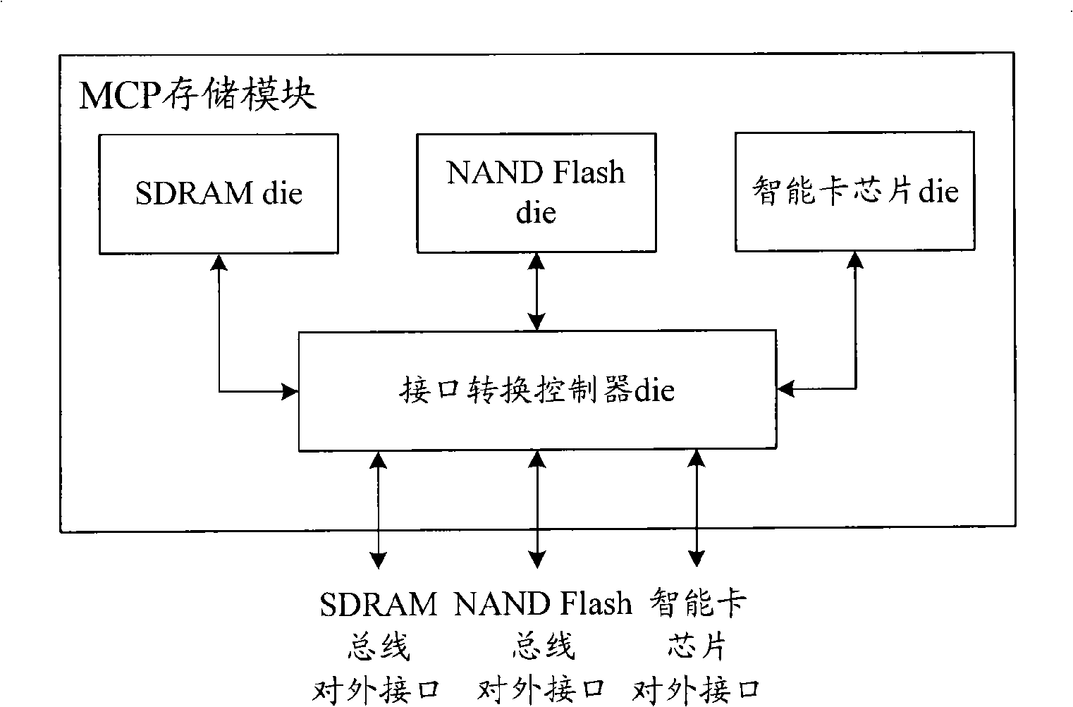
[0105] Figure 9 It is a schematic structural diagram of the MCP storage module in Embodiment 3 of the present invention. Such as Figure 9 As shown, still taking SDRAM and NAND Flash as examples, in Figure 9 middle( image 3 The "die" in represents the die), the SDRAM and NAND Flash in the MCP storage module are connected to the interface conversion controller through the SDRAM bus and the NAND Flash bus respectively, and the smart card chip is connected to the interface conversion controller through the smart card chip bus.

[0106] Such as Figure 9 The MCP storage module shown has two external interfaces, namely SDRAM bus interface and NAND Flash bus interface. The interface conversion controller is connected to the external interface of the SDRAM bus through the SDRAM bus, and is used to establish the communication between the external host and the corresponding type of memory or smart card chip when the external host accesses the corresponding type of memory or smar...


PUM


Abstract

The invention discloses a multi-chip packaging (MCP) memory module. The MCP memory module of the invention not only packages a plurality of types of memorizers for memory but also packages an interface conversion controller and a smart card chip; wherein, the smart card chip can realize relevant safety business of the smart card chip; the interface conversion controller can realize interface specification conversion when the outer part interacts with a plurality of types of memorizers and the smart card chip through an external interface so that the MCP memory module is not limited to the memory function but realizes functional extension. Moreover, the interface conversion controller can realize interface specification conversion, so the external interface arranged on the MCP memory module of the invention can correspond to a plurality of types of memorizers and the smart card chip one by one. Preferably, less external interfaces are needed, e.g. one or two, so that the number of external interface pins of the MCP memory module can be reduced.

Description

technical field [0001] The invention relates to an interface access technology, in particular to a multi-chip package (Multi-Chip Package, MCP) storage module. Background technique [0002] MCP is an advanced integrated circuit packaging process, which uses MCP technology to package various types of memory dies (usually also called bare chips) together to form an MCP memory module. In addition, the MCP memory module has a one-to-one corresponding external interface corresponding to each type of memory die. [0003] Such as figure 1 As shown, the various types of memories packaged in the existing MCP memory module (for ease of expression, the subsequent expressions of this article omit the word "die", and in figure 1 In it, "die" is used to indicate the die) can include: static memory (SRAM) and NAND flash memory (NAND Flash), and the MCP storage module has a corresponding SRAM and an SRAM bus external interface connected to it, and a corresponding NAND Flash and The exter...

Claims


Application Information

Patent Timeline
IPC IPC(8): G11C7/10
Inventor 杨光敏廖泉曹会扬
Owner POTEVIO INFORMATION TECH
Why Eureka
Try Eureka