Data transfer circuit, solid-state imaging device and camera system

A data transmission and data technology, applied in signal transmission system, electrical signal transmission system, TV system scanning details, etc., can solve problems such as difficult to provide driving power, and achieve the effect of reducing delay

Inactive Publication Date: 2008-11-12
SONY CORP
View PDF3 Cites 13 Cited by
  • Summary
  • Abstract
  • Description
  • Claims
  • Application Information

AI Technical Summary

Problems solved by technology

[0006] This is because it is difficult to provide sufficient driving power with an FD amplifier embedded in a pixel

Method used


Image

  • Data transfer circuit, solid-state imaging device and camera system
  • Data transfer circuit, solid-state imaging device and camera system
  • Data transfer circuit, solid-state imaging device and camera system

Examples


Embodiment Construction

[0110] Embodiments of the present invention will be described below with reference to the drawings.

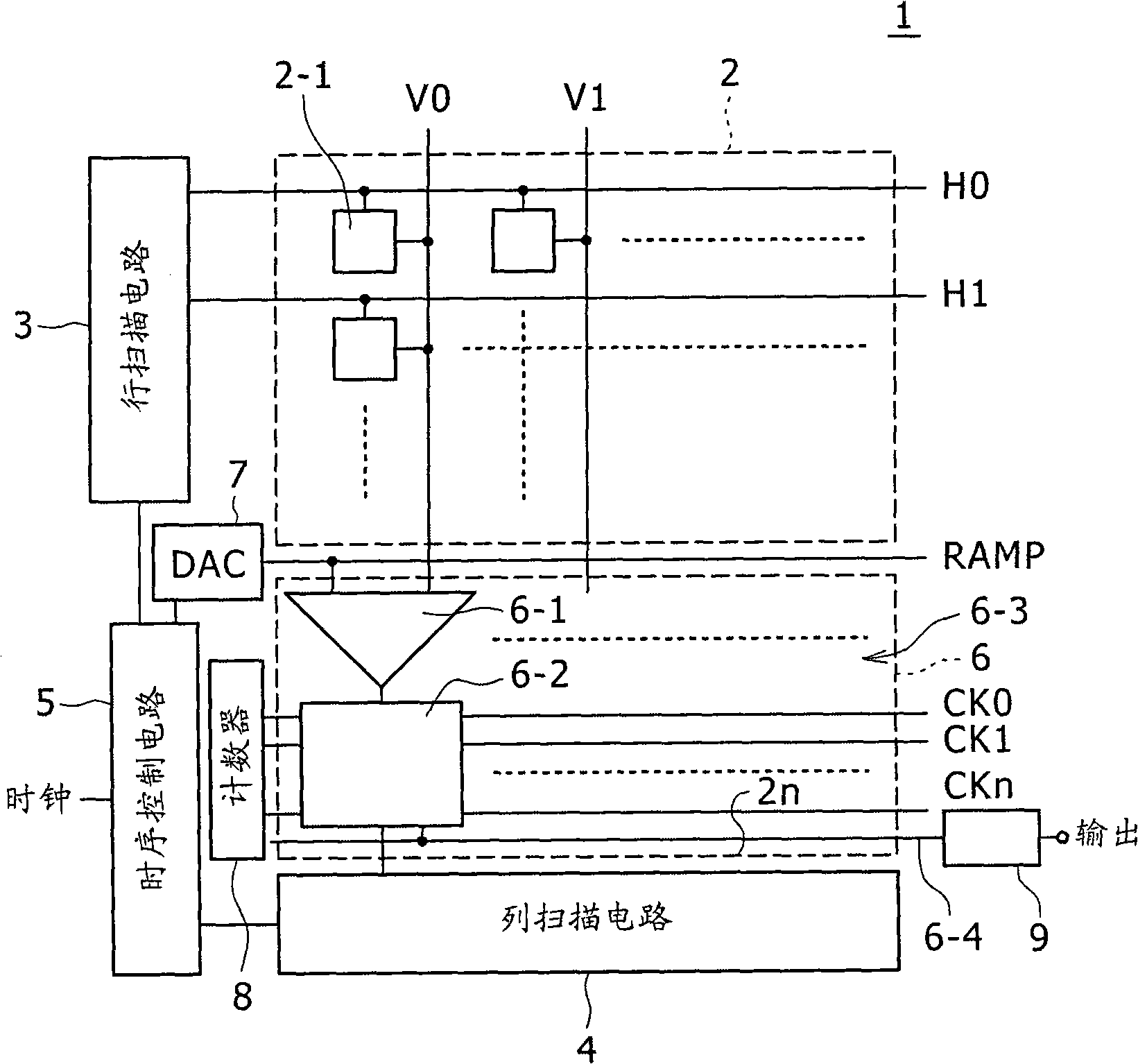
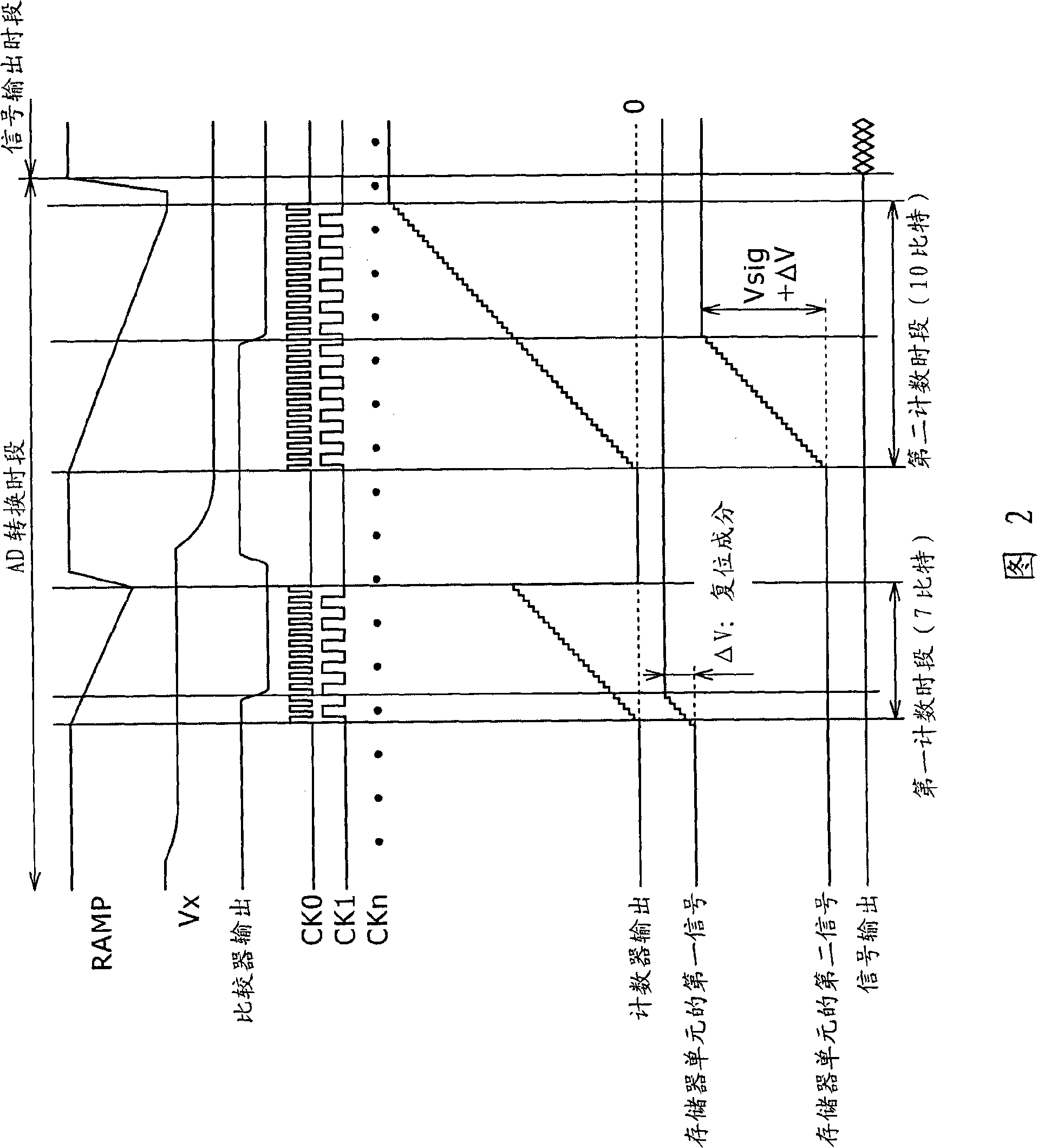
[0111] image 3 is a block diagram showing a typical configuration of an on-a-row-ADC type solid-state imaging device (also called a CMOS image sensor) including a data transfer circuit according to an embodiment of the present invention. Figure 4 is a diagram showing the included image 3 A block diagram of a more specific typical configuration of a data transfer system including a data transfer circuit used in the on-a-row-ADC type solid-state imaging device shown.

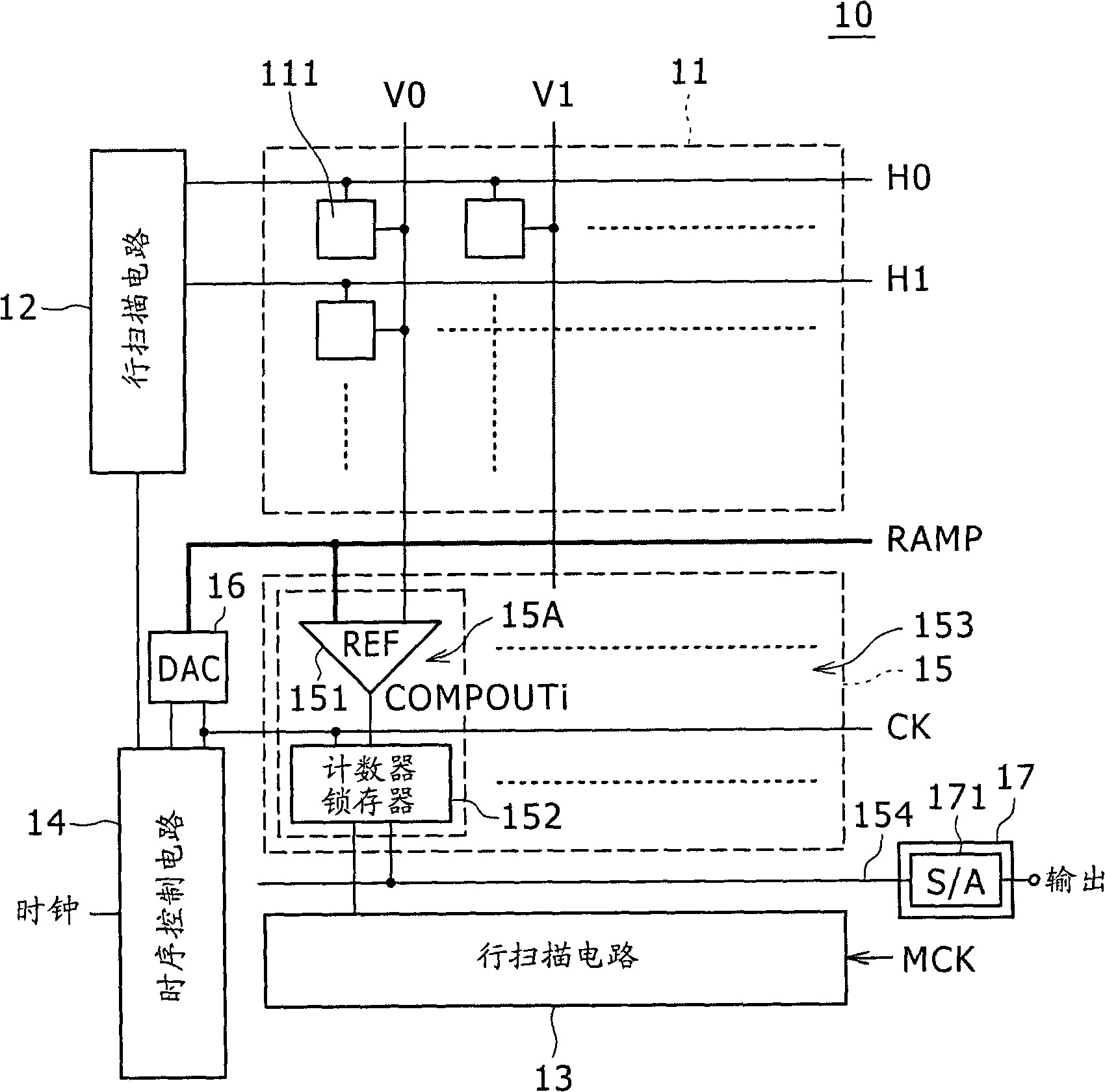
[0112] As shown in FIG. 13, a solid-state imaging device 10 uses a pixel array section 11 serving as an imaging section, a row scanning circuit 12, a column scanning circuit 13, a timing control circuit 14, an ADC group 15, a DAC 16, and each using a sense amplifier ( A plurality of data output circuits (also referred to as data detection circuits) 17 of the S / A) circuit 171 .

[0113] The pixel array section...


PUM


Abstract

Disclosed herein is a data transfer circuit including, a plurality of data transfer lines, a plurality of data outputting sections, a plurality of data holding sections, a data-acquiring-clock supplying section a clock supplying section, and a column scan section.

Description

technical field [0001] The present invention relates to a data transmission circuit, a solid-state imaging device typified by a CMOS image sensor, and a camera system. Background technique [0002] In recent years, CMOS image sensors have attracted attention as solid-state imaging devices used as image sensors replacing CCDs. [0003] This is because special handling is required in constructing the CCD pixel, and in addition, multiple power supply voltages are required in order to operate the CCD pixel. Based on this, in the case of a CCD, it is necessary to combine a plurality of peripheral chips and operate the chip. A CMOS image sensor is therefore used as a sensor for solving various problems each arising in a CCD pixel-based system as a problem that complicates the system. [0004] CMOS image sensors can be constructed using the same manufacturing processes as those used to construct general CMOS integrated circuits. In addition, a CMOS image sensor can be driven by ...

Claims


Application Information

Patent Timeline
Patent Type & Authority Applications(China)
IPC IPC(8): H04N3/15H04N5/335H03M1/46H04N5/341H04N5/369H04N5/374
CPCH04N25/772H04N25/778H04N25/771H04N25/745
Inventor 田口宏幸岩城宏行小关贤藤原明子寺笼博裕松永宪市藤田幸生
Owner SONY CORP
Why Eureka
Try Eureka