Liquid crystal display panel and method for making the same

A technology for liquid crystal display panels and substrates, which is applied in the photoengraving process, optics, optomechanical equipment and other directions of the pattern surface, which can solve the problems of complicated processes and high material costs, improve the allowable range, reduce costs, and reduce materials and processes. cost effect

Active Publication Date: 2008-12-24
AU OPTRONICS CORP
View PDF0 Cites 14 Cited by
  • Summary
  • Abstract
  • Description
  • Claims
  • Application Information

AI Technical Summary

Problems solved by technology

Although the liquid crystal display panel 20 only needs one photolithography process to form the photoresist spacers 28, an additional process is still required to form the metal matrix layer 30, so the liquid crystal display panel 20 still has the disadvantage of complicated processes.
[0005] In addition, traditional photoresist spac

Method used


Image

  • Liquid crystal display panel and method for making the same
  • Liquid crystal display panel and method for making the same
  • Liquid crystal display panel and method for making the same

Examples


Example Embodiment

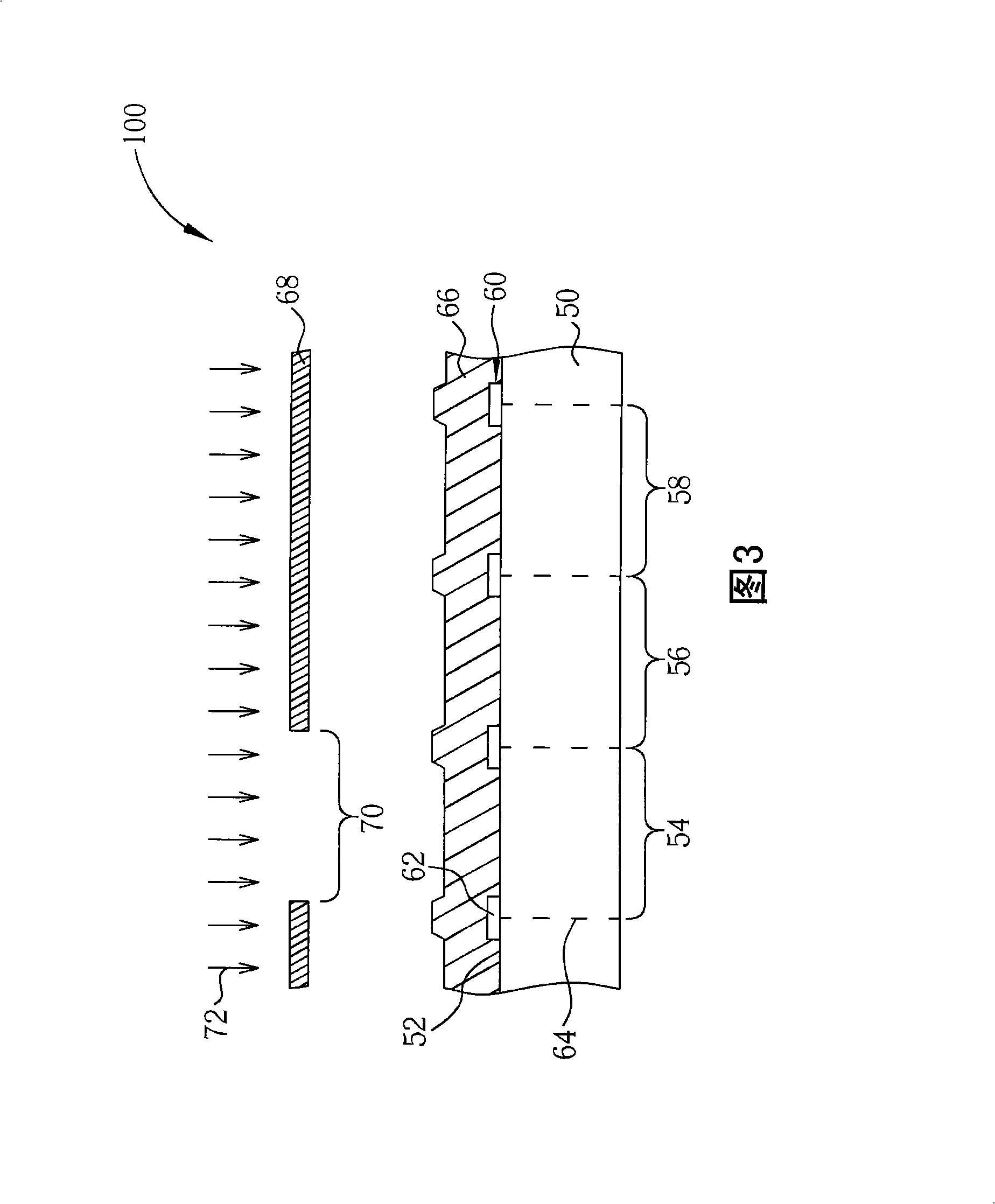
[0053] Please refer to FIGS. 3 to 8. FIGS. 3 to 8 are schematic cross-sectional views of the first embodiment of the method for manufacturing a liquid crystal display panel of the present invention. FIG. 3 is a partially enlarged schematic diagram of the first substrate 50 of the liquid crystal display panel 100 of the present invention. According to the manufacturing method of the present invention, first, a first substrate 50 is provided, which includes a plurality of first sub-pixel regions 54, a plurality of second sub-pixel regions 56, and a plurality of third sub-pixel regions 58, which are arranged adjacent to each other to form a matrix arrangement. The first sub-pixel area 54, the second sub-pixel area 56, and the third sub-pixel area 58 respectively represent sub-pixels that can provide light of different or the same color. Next, a patterned black matrix layer 60 is formed on the first surface 52 of the first substrate 50, which includes a plurality of black matrix patte...


PUM


Abstract

The invention provides a liquid crystal display panel and a production method thereof, wherein, the liquid crystal display panel comprises a first substrate, a second substrate, a liquid crystal layer arranged between the first substrate and the second substrate, a patterned black matrix layer arranged on the surface of the first substrate, a patterned first color filter layer arranged on the surface of the first substrate, a plurality of first spherical spacers and a plurality of second spherical spacers, wherein, the protruding part of the patterned first color filter layer covers part of the patterned black matrix layer. The first spherical spacers are arranged on the surface of the patterned black matrix layer, the second spherical spacers are arranged on the surface of the protruding part of the patterned first color filter layer, the bottom surfaces of the second spherical spacers and the bottom surfaces of the first spherical spacers are positioned on the different planes in the liquid crystal display panel. The liquid crystal display panel can improve the allowable range of the liquid crystal filling amount.

Description

Technical field [0001] The present invention relates to a liquid crystal display panel and a manufacturing method thereof, and more particularly to a liquid crystal display panel including a hybrid ball spacer structure and a manufacturing method thereof. Background technique [0002] With the development of liquid crystal display technology becoming more and more mature, liquid crystal display devices have been widely used in various information products, such as portable information products such as notebook computers, personal digital assistants, and mobile phones, and have even gradually replaced traditional cathode ray tube displays. The main components of the liquid crystal display device include a liquid crystal display panel, which includes two transparent substrates and a liquid crystal layer arranged between the transparent substrates, and the gap between the transparent substrates is maintained through a sealant and a spacer. The current commonly used liquid crystal fi...

Claims


Application Information

Patent Timeline
IPC IPC(8): G02F1/1339G02F1/1333G03F7/00
Inventor 朱智伟谢明哲王世育
Owner AU OPTRONICS CORP
Why Eureka
Try Eureka