Multi- domain LCD device

A liquid crystal display and liquid crystal layer technology, which is applied to instruments, nonlinear optics, optics, etc., can solve the problems of reducing the overall light transmittance, insufficient liquid crystal molecules 208, discontinuous misalignment defects, etc., to avoid light leakage and coupling. Small capacitance effect, the effect of avoiding voltage offset

Inactive Publication Date: 2010-06-02
WINTEK CORP +1
View PDF6 Cites 0 Cited by
  • Summary
  • Abstract
  • Description
  • Claims
  • Application Information

AI Technical Summary

Problems solved by technology

However, the way to form the slit 206 at the electrode 204 must carefully consider the width of the slit 206 itself and the distance between the two slits 206, or the force generated by the slit 206 to cause the liquid crystal molecules 208 to fall is easily insufficient.
Furthermore, the design of the slit 206 causes the energy of the liquid crystal molecules 208 to rotate in either direction to be equal, so that the alignment distribution of the liquid crystal molecules 208 in space produces discontinuous disclination.
The misalignment defect region 210 is easily formed above the slit 206 and between the two slits 206, thereby reducing the overall light transmittance

Method used


Image

  • Multi- domain LCD device
  • Multi- domain LCD device
  • Multi- domain LCD device

Examples


Embodiment Construction

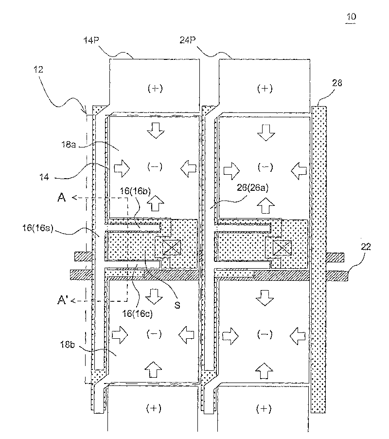
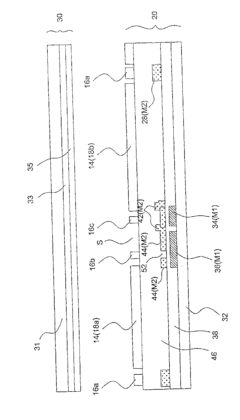
[0051] figure 1 and figure 2 According to an embodiment of the present invention, it shows a schematic diagram of a multi-domain liquid crystal display 10, wherein figure 1 is a top view viewed from the normal direction of the array substrate, figure 2 for along figure 1 The cross-sectional view obtained by cutting the A-A' line.

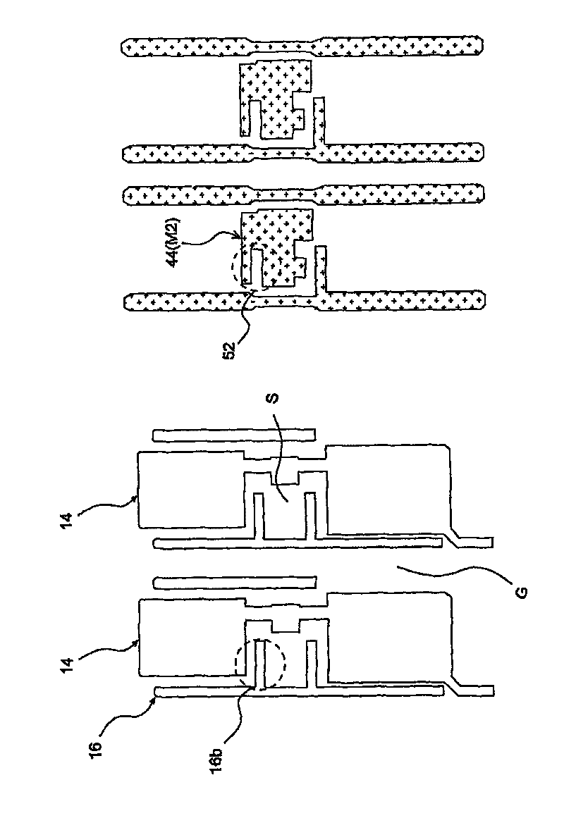
[0052] Such as figure 1As shown, the multi-domain liquid crystal display 10 includes a plurality of pixel units 12. According to the design of this embodiment, a pixel electrode 14 and an auxiliary electrode 16 are formed in a pixel unit 12, and each auxiliary electrode disposed on the side of the pixel electrode 14 16 is electrically connected to the pixel electrode 14P controlled by the previous scan line (not shown). Furthermore, the non-display area formed by the opaque components such as thin film transistors and storage capacitors is located in the central part of a pixel unit 12, and the display area of ​​the pixel unit 12 is divid...


PUM


Abstract

A multi-domain liquid crystal display comprises two transparent substrates, a liquid crystal layer disposed therebetween, a common electrode, a first metal layer, a first dielectric layer, a second metal layer, a second dielectric layer, a plurality of pixel electrodes, and a plurality of auxiliary electrodes. The first dielectric layer is formed on the second transparent substrate and covers thefirst metal layer, the second metal layer is formed on the first dielectric layer, and the second dielectric layer is formed on the first dielectric layer and covers the second metal layer. The plurality of pixel electrodes are formed on the second dielectric layer, each being provided with at least one opening extending inwardly from the fringe so as to be partitioned into a plurality of blocks.The plurality of auxiliary electrodes are formed on the second dielectric layer, each being adjacent to at least one side of one pixel electrode block while being at least distributed inside the opening of the pixel electrode to form a fringe field, and at least one opening is formed at a position where the second metal layer laminating the auxiliary electrodes.

Description

technical field [0001] The invention relates to a liquid crystal display with multi-domain alignment. Background technique [0002] The existing liquid crystal alignment method using negative type liquid crystal material with negative dielectric anisotropy to form vertical alignment (vertical alignment), because the liquid crystal molecules are arranged vertically to the substrate when no voltage is applied, it can provide good Contrast performance. However, in order to form a multi-domain splitting effect in a vertically aligned LCD, the matching structure may have some light leakage or insufficient multi-domain splitting configuration capability. [0003] Figure 11A It is a schematic cross-sectional view showing the design of a conventional multi-domain vertically aligned LCD (MVA LCD). Such as Figure 11A As shown, bumps 106 are respectively formed on the upper and lower substrates 102, 104, and a vertical alignment film 108 covering the bumps 106 is formed on the uppe...

Claims


Application Information

Patent Timeline
Patent Type & Authority Patents(China)
IPC IPC(8): G02F1/1333G02F1/1343G02F1/1362
Inventor 王文俊刘锦璋
Owner WINTEK CORP
Why Eureka
Try Eureka