Thin-film transistor array substrate

A thin-film transistor and array substrate technology, which is applied in the field of thin-film transistor array substrates, can solve the problems of reducing light transmittance, discontinuous misdirection defects, etc., and achieve the effects of avoiding light leakage, strong dumping force, and small aperture ratio

Inactive Publication Date: 2010-12-08
WINTEK CORP
View PDF5 Cites 0 Cited by
  • Summary
  • Abstract
  • Description
  • Claims
  • Application Information

AI Technical Summary

Problems solved by technology

like Figure 10 As shown, the slit 206 formed on the transparent electrode 204 of the substrate 202 can control the tilting direction of the liquid crystal molecules 208 after the voltage is applied. However, the method of forming the slit 206 at the electrode 204 must be carefully Consider the width of the slit 206 itself and the distance between the two slits 206, etc. Otherwise, the force generated by the slit 206 to cause the liquid crystal molecules 208 to fall is easily insufficient. Furthermore, the design of the slit 206 will cause the liquid crystal molecules 208 to fall. The energy of rotation in any direction of the left and right is equal, so that the alignment distribution of the liquid crystal molecules 208 in space produces discontinuous dislocation defects (disclination). formed, while reducing the overall light transmittance

Method used


Image

  • Thin-film transistor array substrate
  • Thin-film transistor array substrate
  • Thin-film transistor array substrate

Examples


Embodiment Construction

[0048] The aforementioned and other technical contents, features and functions of the present invention will be clearly presented in the following detailed description of the embodiments with reference to the drawings. The directional terms mentioned in the following embodiments, such as: up, down, left, right, front or back, etc., are only directions referring to the attached drawings. Accordingly, the directional terms are used to illustrate and not to limit the invention.

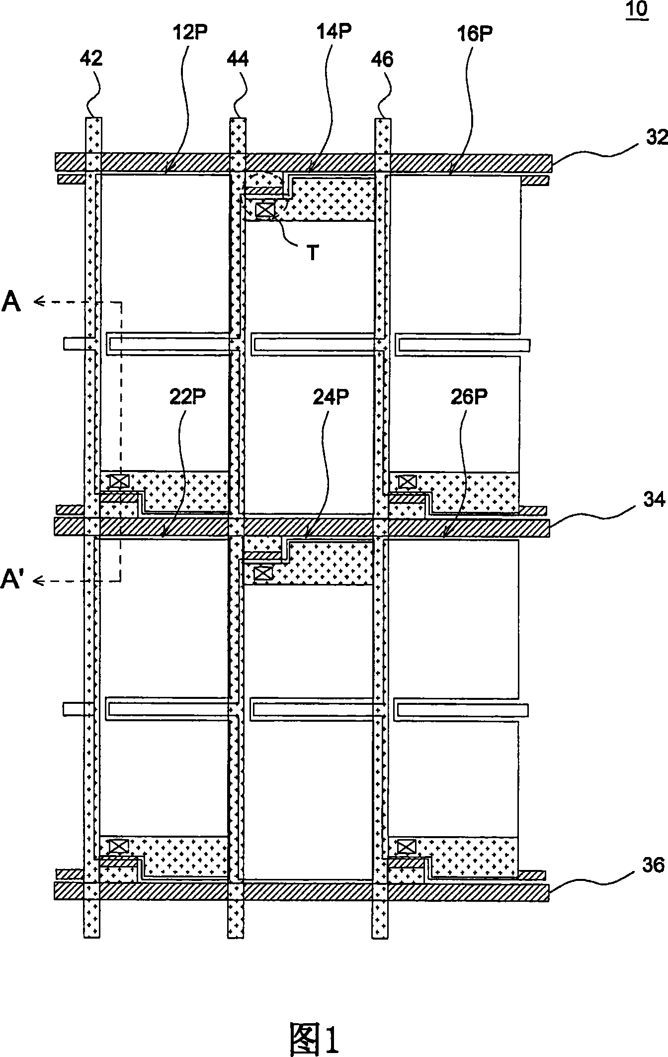
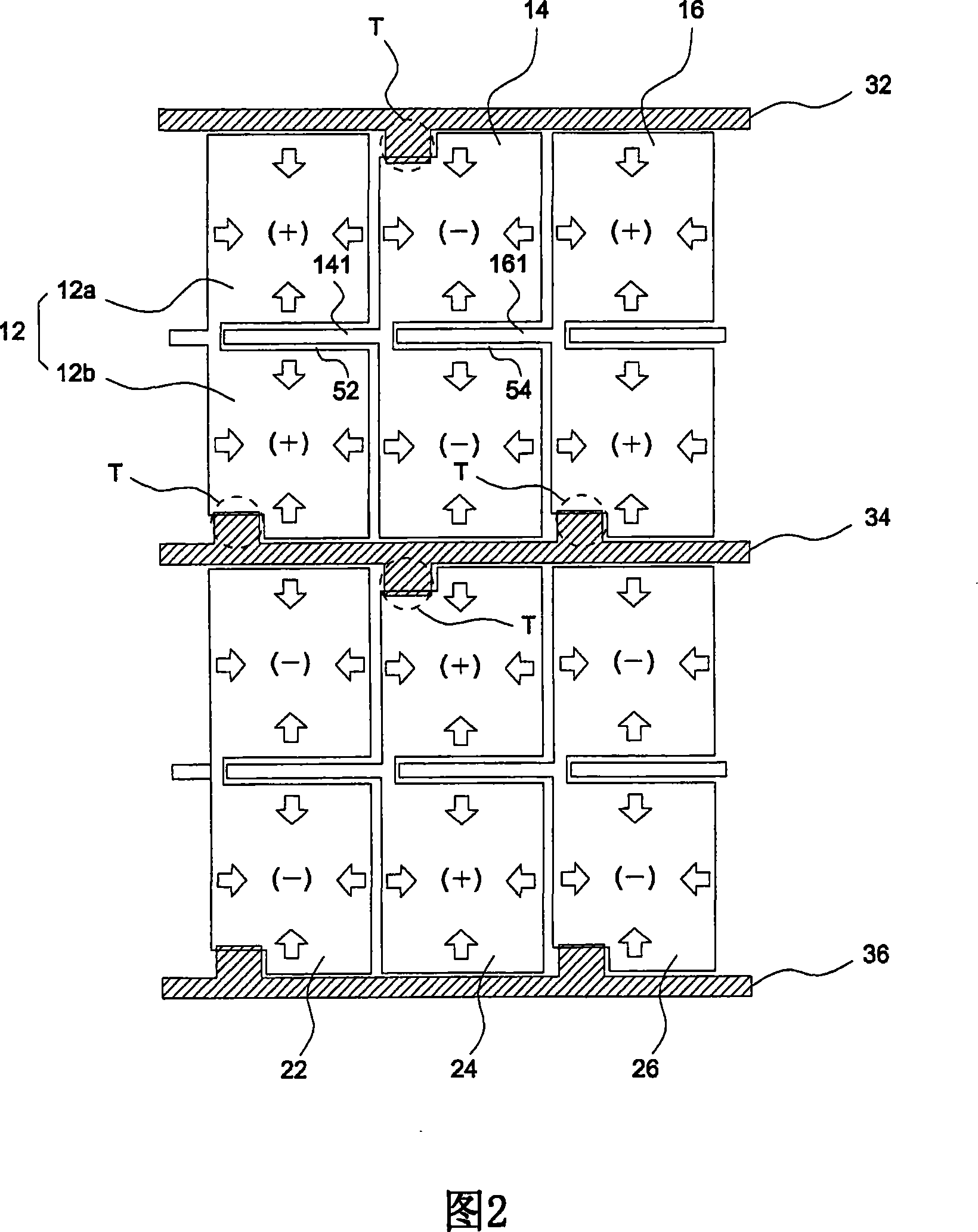
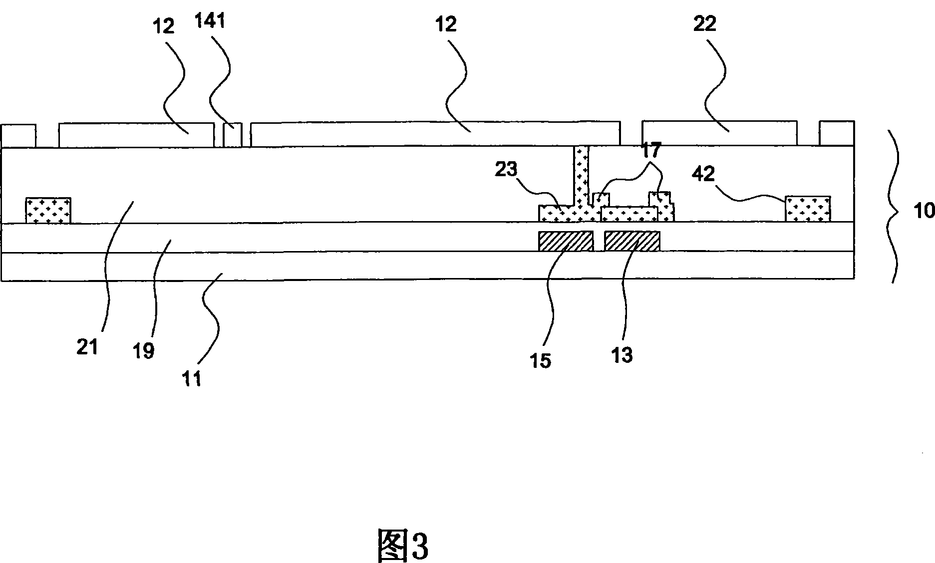
[0049] figure 1 According to an embodiment of the present invention, a schematic plan view of a thin film transistor array substrate 10 is shown. Such as figure 1As shown, a plurality of scan lines 32, 34, 36 parallel to each other and data lines 42, 44, 46 parallel to each other are formed on an insulating substrate (not shown), and two adjacent scan lines are orthogonal to the two phases. Adjacent data lines encircle a pixel unit distribution area, such as the active element of thin film transisto...


PUM


Abstract

The invention relates to a thin-film transistor array substrate including an insulation substrate, a plurality of scan lines, a data wire and a pixel unit. The plural pixel units matching with the scan lines and the data wire divide each pixel unit and define a row direction and a column direction. Each pixel unit comprises a thin-film transistor eclectically connected to the scan lines and data wire and a pixel electrode having at least an opening extending from the edge to the internal and an extending part extending along the column direction. The extending part of the pixel electrode extends into another pixel electrode opening adjacent to the column direction, and the same scan line intervally controls the pixel unit along the column direction. The thin-film transistor substrate of the invention can obtain good multi-domain effect by using a simplified drive architecture and lower cost.

Description

technical field [0001] The invention relates to a thin film transistor array substrate with multi-domain alignment effect. Background technique [0002] The existing liquid crystal alignment method using negative type liquid crystal material with negative dielectric anisotropy to form vertical alignment (vertical alignment), because the liquid crystal molecules are arranged vertically to the substrate when no voltage is applied, it can provide good However, in order to form a multi-domain split effect in a vertically aligned LCD, the matching structure may have some light leakage or insufficient multi-domain split configuration capability. [0003] Figure 8 It is a schematic cross-sectional view showing the design of a conventional multi-domain vertically aligned LCD (MVA LCD). Such as Figure 8 As shown, bumps 106 are respectively formed on the upper and lower substrates 102, 104, and a vertical alignment film 108 covering the bumps 106 is formed on the upper and lower su...

Claims


Application Information

Patent Timeline
Patent Type & Authority Patents(China)
IPC IPC(8): H01L27/12H01L23/522G02F1/1362
Inventor 王文俊刘锦璋王义方
Owner WINTEK CORP
Why Eureka
Try Eureka