Liquid crystal display panel and pixel structure thereof

A liquid crystal display panel and pixel structure technology, applied in nonlinear optics, instruments, optics, etc., can solve the problems of increased manufacturing process cost, decreased aperture ratio, light leakage, etc., achieve the best overall alignment effect, reduce size, and increase aperture ratio Effect

Active Publication Date: 2010-06-02
AU OPTRONICS CORP
View PDF4 Cites 0 Cited by
  • Summary
  • Abstract
  • Description
  • Claims
  • Application Information

AI Technical Summary

Problems solved by technology

[0004] The known pixel structure 10 using alignment bumps 24 for alignment has the following disadvantages: first, the manufacturing process of the second substrate 14 must be increased to make the alignment bumps 24, which will increase the cost of the manufacturing process; secondly, light leakage will occur around the alignment bumps 24 , and black light-shielding pattern 26 must be set for light-shielding, and in order to effectively shield light leakage, the size of black light-shielding pattern 26 must be larger than the size of alignment bump 24, thus causing the aperture ratio to decrease; in addition, the production of alignment bump 24 is limited by manufacturing The minimum size is limited by the process limit, so in the high-resolution liquid crystal display panel, the existence of the alignment bump 24 will also cause the aperture ratio to decrease

Method used


Image

  • Liquid crystal display panel and pixel structure thereof
  • Liquid crystal display panel and pixel structure thereof
  • Liquid crystal display panel and pixel structure thereof

Examples


Embodiment Construction

[0032] In order to enable those of ordinary skill who are familiar with the technical field of the present invention to further understand the present invention, several preferred embodiments of the present invention are enumerated below, and in conjunction with the attached drawings, the constitutional content and the desired achievement of the present invention are explained in detail. Effect.

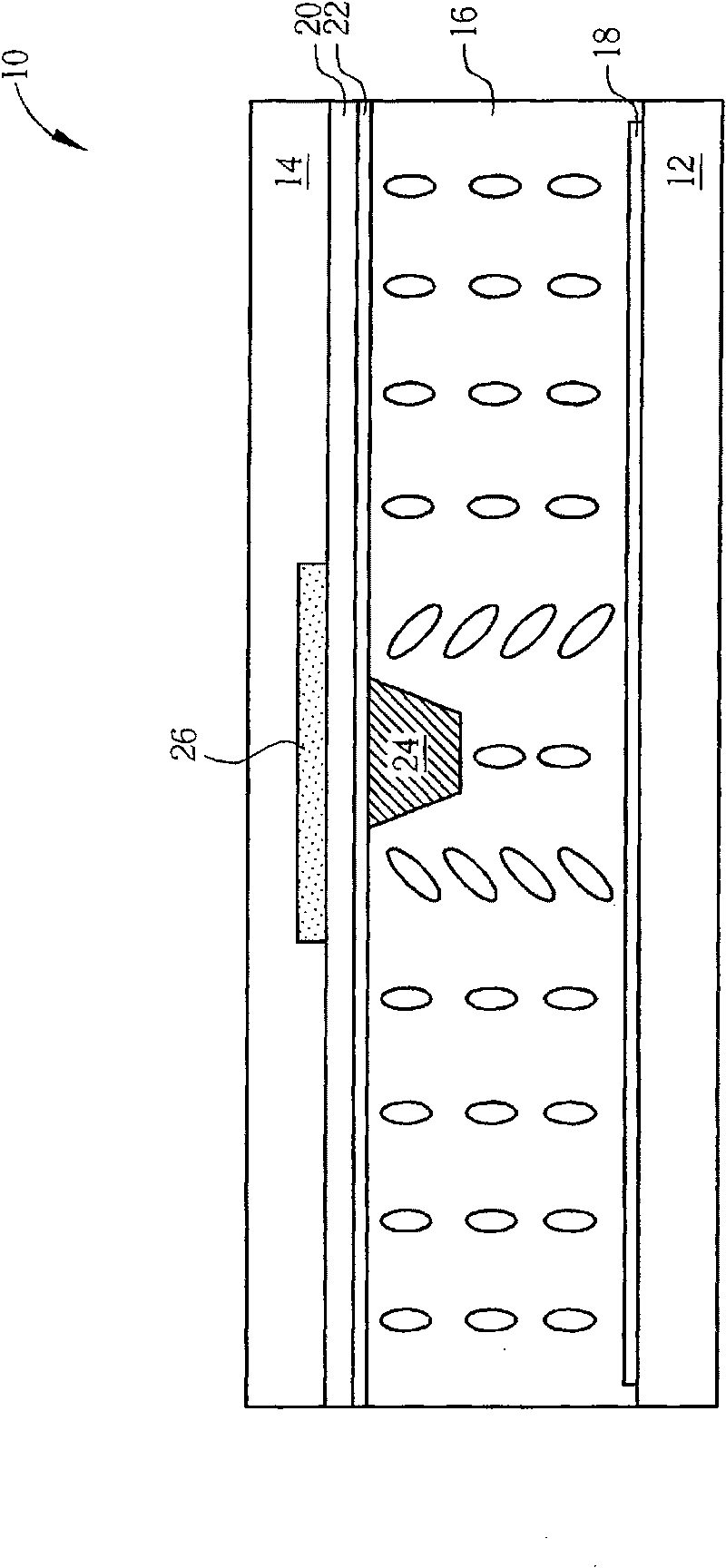
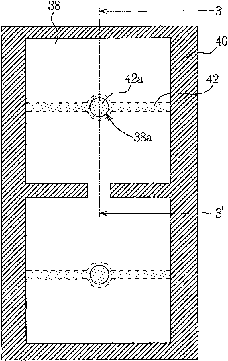
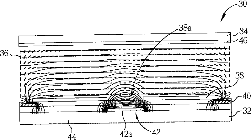
[0033] Please refer to figure 2 and image 3 . figure 2 and image 3 is a schematic diagram of the first preferred embodiment of the pixel structure of the liquid crystal display panel of the present invention, wherein figure 2 For a top view, image 3 for along figure 2 In order to clearly show the features of the present invention, only a single pixel structure of the liquid crystal display panel is shown in the figure, and the description below will be described with a single pixel structure. like figure 2 and image 3 As shown, the liquid crystal display panel of thi...


PUM


Abstract

The invention provides a dot structure, comprising at least an pixel electrode and at least an aligning electrode; the pixel electrode is arranged on a substrate; furthermore, the pixel electrode is provided with a central opening; the aligning electrode is arranged between the pixel electrode and the substrate and comprises an aligning part which is arranged below the central opening and corresponding to the central opening; the aligning voltage of the aligning electrode is more than the pixel voltage of the pixel electrode. The dot structure of the liquid crystal display panel of the invention uses the aligning electrode to carry out the multi-area alignment, thereby requiring no aligning bulges. Furthermore, the dot structure uses a first common electrode to carry out the alignment of the edge of the dot structure, thereby having extremely good whole aligning effect and quick response time; furthermore, the arrangement of the first common electrode can shorten the dimension of the aligning electrode and improve the aperture opening ratio of the dot structure; furthermore, the manufacture process limit of the aligning electrode and the pixel electrode is higher than the manufacture process limit of the aligning bulge; therefore, when the aligning electrode is arranged in the high-resolution liquid crystal display panel, the resolution is not affected.

Description

technical field [0001] The invention relates to a liquid crystal display panel and its pixel structure, in particular to a pixel structure of a multi-region vertical alignment type liquid crystal display panel provided with alignment electrodes. Background technique [0002] Liquid crystal displays have been widely used in various electronic products, such as mobile phones, personal digital assistants and notebook computers, etc., and with the rapid development of large-scale thin flat-screen TVs, LCD TVs with thin, light and small features play a very important role. role, and gradually replaced the cathode ray tube (CRT) TV as the mainstream of thin flat-screen TVs. However, due to the congenital defect of the narrow viewing angle of the liquid crystal display panel, which has become a restriction condition for its development, a multi-domain vertical alignment (MVA) liquid crystal display panel with a wide viewing angle has been developed accordingly. [0003] Please ref...

Claims


Application Information

Patent Timeline
Patent Type & Authority Patents(China)
IPC IPC(8): G02F1/1343G02F1/1337G02F1/139
Inventor 刘松高林祥麟林敬桓胡至仁
Owner AU OPTRONICS CORP
Why Eureka
Try Eureka