
Expansion of a stacked register file using shadow registers
A technology of register files and registers, which is applied in the direction of instruments, machine execution devices, calculations, etc., can solve the problems of high cost, low utilization rate of high-cost hardware, and increase of physical register files 1, etc.
- Summary
- Abstract
- Description
- Claims
- Application Information
AI Technical Summary
Problems solved by technology
Method used
Image

Examples
Embodiment Construction
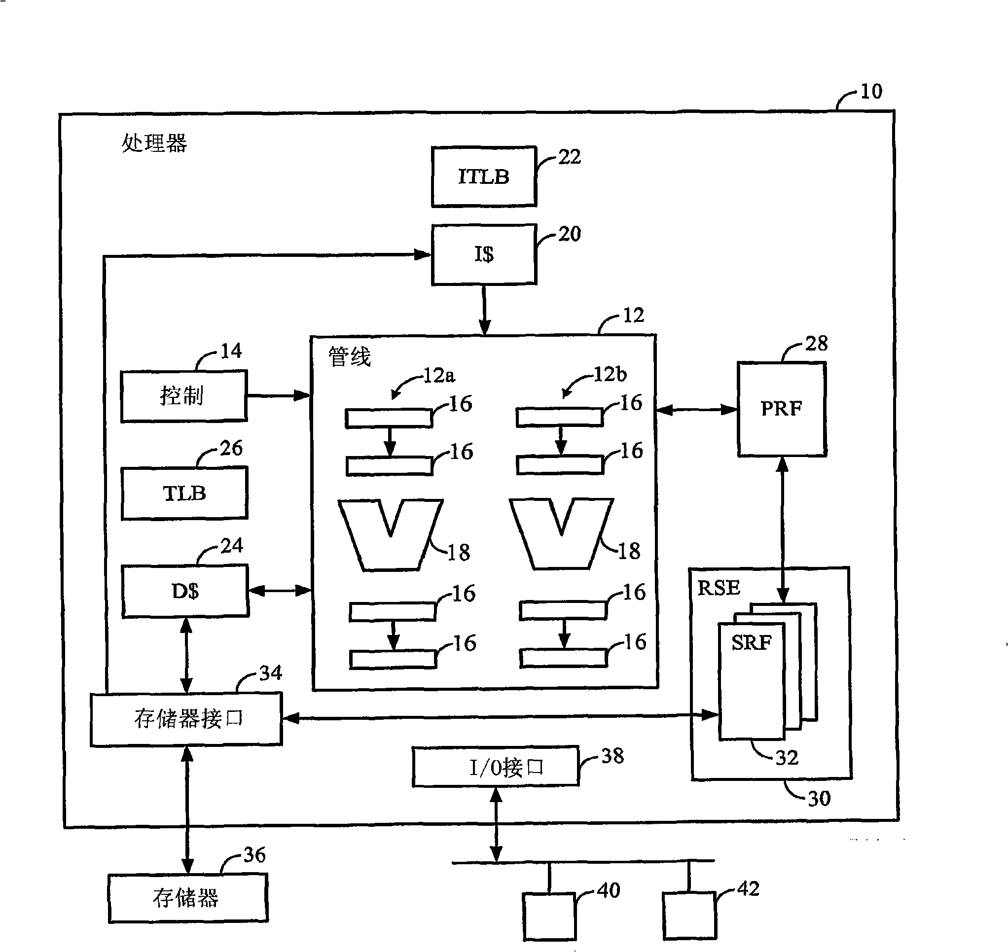
[0021] figure 2A functional block diagram of processor 10 is depicted. The processor 10 executes the instructions in the instruction execution pipeline 12 according to the control logic 14 . Pipeline 12 may be a superscalar design, with multiple parallel pipelines, such as 12a and 12b. Each pipeline 12a, 12b includes various registers or latches 16 organized into stages, and one or more arithmetic logic units (ALUs) 18 . Pipelines 12a, 12b fetch instructions from an instruction cache (I-cache or I$) 20 where memory addressing and permissions are managed by an instruction-side translation lookaside buffer (ITLB) 22 .
[0022] Data is accessed from a data cache (D-cache or D$) 24 where memory addressing and permissions are managed by a main translation lookaside buffer (TLB) 26 . In various embodiments, ITLB 22 may include a replica of a portion of TLB 26 . Alternatively, ITLB 22 and TLB 26 may be integrated. Similarly, in various embodiments of processor 10, I-cache 20 and...
PUM
 Abstract
Description
Claims
Application Information