
Method for manufacturing position phase array machine capable of adjusting two-dimensional photon microstructure

A technology of photonic microstructure and manufacturing method, which is applied in the field of optical communication and optical multi-channel imaging, can solve the problems of difficult array light emission and difficult manufacturing process, etc., and achieve the effect of simplifying the processing process

Inactive Publication Date: 2009-02-25
BEIJING JIAOTONG UNIV
View PDF0 Cites 10 Cited by
  • Summary
  • Abstract
  • Description
  • Claims
  • Application Information

AI Technical Summary

Problems solved by technology

The present invention overcomes the disadvantages that the current phase array device manufactured by commonly used micro-optical array elements can only correspond to a specific wavelength, it is difficult to realize the array light emission of any wavelength within the light transmission range of the substrate, and the manufacturing process is difficult

Method used


Image

  • Method for manufacturing position phase array machine capable of adjusting two-dimensional photon microstructure
  • Method for manufacturing position phase array machine capable of adjusting two-dimensional photon microstructure

Examples


Embodiment Construction

[0023] The preferred embodiments will be described in detail below in conjunction with the accompanying drawings. It should be emphasized that the following description is only exemplary and not intended to limit the scope of the invention and its application.

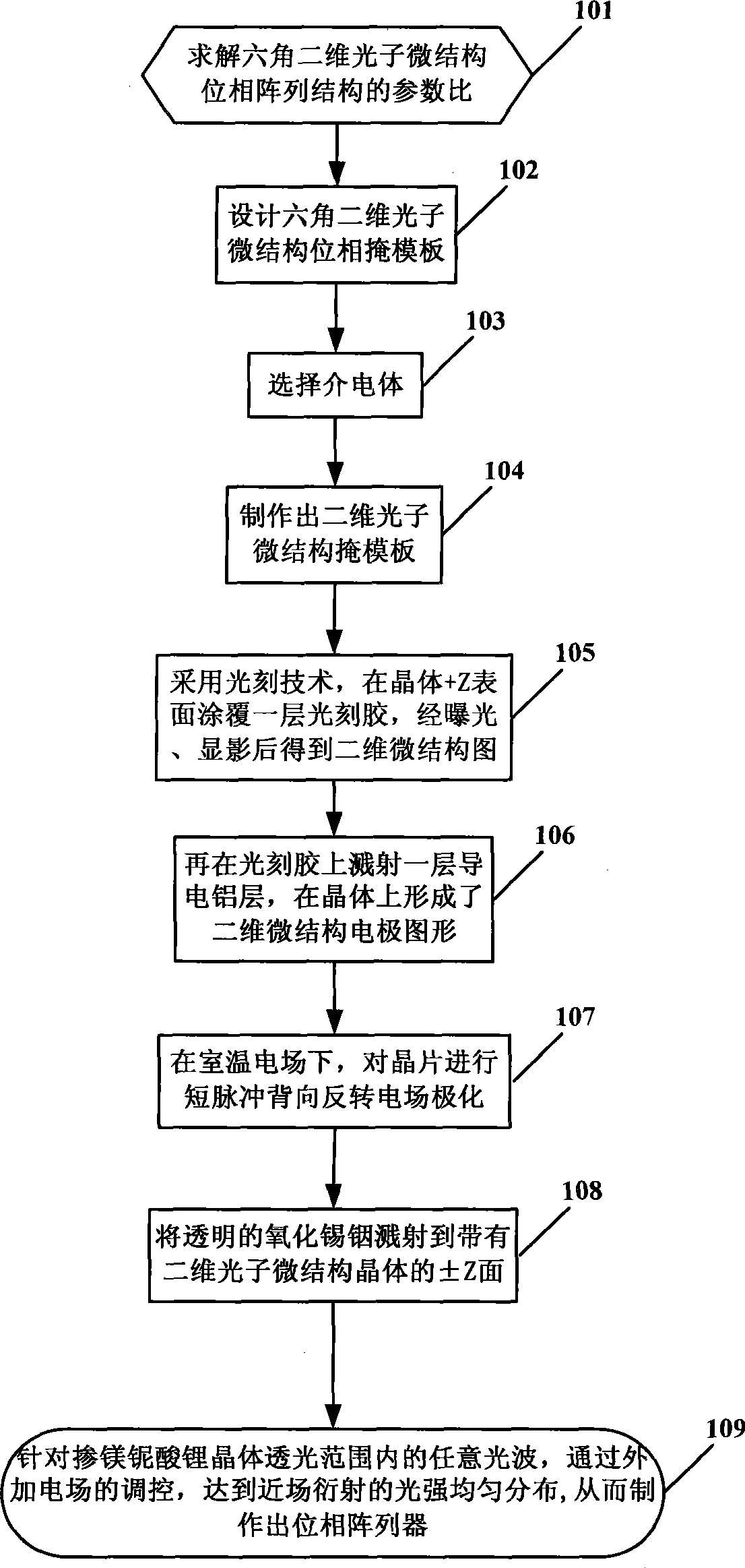
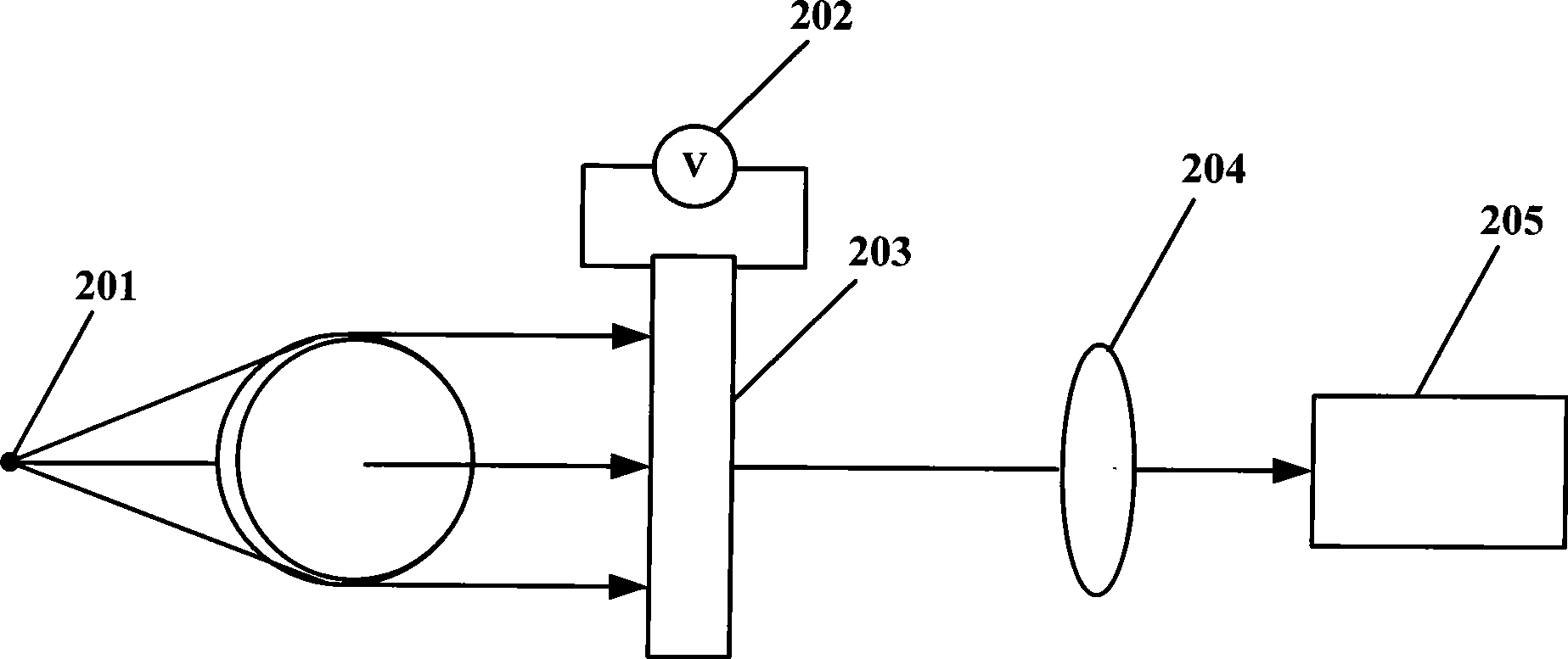
[0024] figure 1 It is a flowchart of a manufacturing method of an adjustable two-dimensional photonic microstructure phase array device. figure 1 In step 101, analyze and numerically simulate the complex amplitude distribution of the light wave and the complex amplitude distribution of the hexagonal two-dimensional photonic microstructure light array on the planes with different Talbot distances, and numerically solve the hexagonal two-dimensional photonic microstructure phase array structure theoretically. Parameter ratio dx / dy. According to the principle of light wave reversibility, if the phase array is made according to the periodic distribution of its phase, then under the illumination of light wave, an array im...


PUM


Abstract

The invention discloses a manufacturing method for an adjustable two-dimensional photon microstructure phase array device, and belongs to the technical fields of optical communication and optical multi-path imaging. The technical proposal is that the hexangular two-dimensional photon microstructure phase array can be manufactured on a substrate of LiNbO3 crystals doped with Mg by utilizing the mature semiconductor photoetching technique process and adopting the trailing direction reversion burst pulse polarization electric field technique. The LiNbO3 crystals doped with Mg has better electro-optical properties, so that through the regulation and the control of an external electric field added on the plus or minus Z surface of the substrate with the two-dimensional photon microstructure, the continuous change of the phase between 0 to 2Pi can be realized, and a random light wave within the transmission range (5Mum-320nm) of the LiNbO3 crystals doped with Mg can realize the phase period distribution field to enable the light intensity of near field diffraction to be distributed uniformly. Through using the LiNbO3 crystals doped with Mg, the invention can direct process and manufacture micro-optical array elements, thereby realizing the array irradiancy of the random light wave within the transmission range of the crystals, and simplifying the manufacturing procedure at the same time.

Description

technical field [0001] The invention belongs to the technical field of optical communication and optical multi-channel imaging, and in particular relates to a manufacturing method of an adjustable two-dimensional photonic microstructure phase array device. Background technique [0002] With the rapid development of science and technology and modern national defense, it is increasingly required to develop miniaturized, arrayed and multifunctional optical devices and systems. For example, in the fields of optical communication, optical and electronic computing technology, and image processing, it is necessary to use various micro-optical devices to realize parallel transmission and processing of information, thereby increasing the speed. In systems such as optical computing, optical neural network, and optical multi-channel imaging, it is often required to form a group of light arrays on the output plane with a beam of incident light, and the light intensity in the array is un...

Claims


Application Information

Patent Timeline
IPC IPC(8): G02F1/03G03F7/00
Inventor 陈云琳周波
Owner BEIJING JIAOTONG UNIV
Learn More