

Mask for semiconductor device and patterning method using the same
A pattern and mask technology, applied in the field of masks of semiconductor devices, can solve problems such as difficulty in optimizing the optical proximity correction pattern 10
- Summary
- Abstract
- Description
- Claims
- Application Information
AI Technical Summary
Problems solved by technology
Method used
Image

Examples
Embodiment Construction
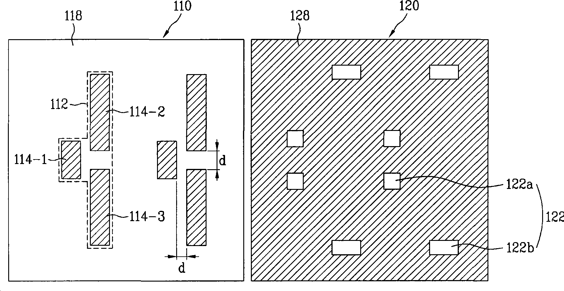
[0021] Exemplary figure 2 is a plan view of a mask of a semiconductor device according to an embodiment of the present invention. see example figure 2 , the mask includes a first mask 110 and a second mask 120 , the first mask 110 includes a main pattern 112 , and the second mask 120 includes an auxiliary pattern 122 . The first mask 110 includes a light shielding region and a light transmissive region 118 on which a plurality of split patterns 114-1, 114-2, and 114 are formed. -3, the light-transmitting region 118 is other regions except the light-shielding region. More specifically, the light-shielding region includes a light-shielding layer formed on a substrate of the mask. The separated patterns 114-1, 114-2, and 114-3 serve to prevent light transmission. The light transmissive area 118 includes a mask substrate that allows light to transmit.
[0022] A plurality of separate patterns 114 - 1 , 114 - 2 and 114 - 3 together constitute the main pattern 112 . Each of ...
PUM
 Abstract
Description
Claims
Application Information