

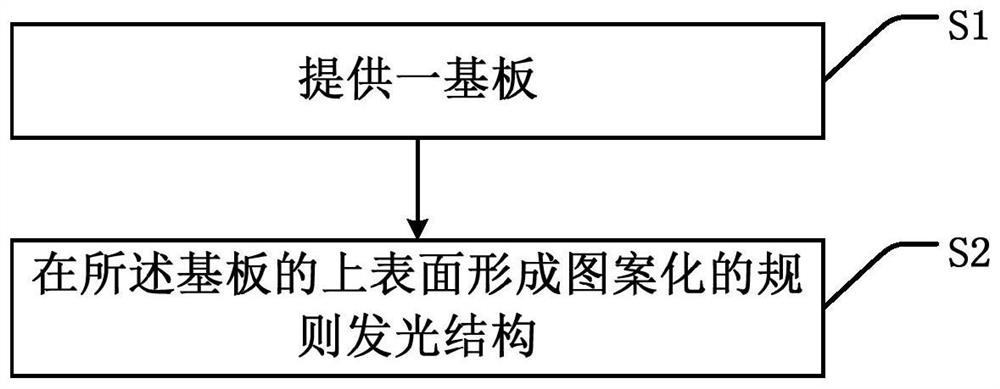
Perovskite light-emitting film layer, preparation method thereof and display panel
A perovskite and light-emitting film technology, which is applied in semiconductor/solid-state device manufacturing, semiconductor devices, electrical components, etc., can solve the problems of poor patterning effect of the light-emitting layer and achieve precise patterning effect
- Summary
- Abstract
- Description
- Claims
- Application Information
AI Technical Summary
Problems solved by technology
Method used
Image

Examples
Embodiment 1
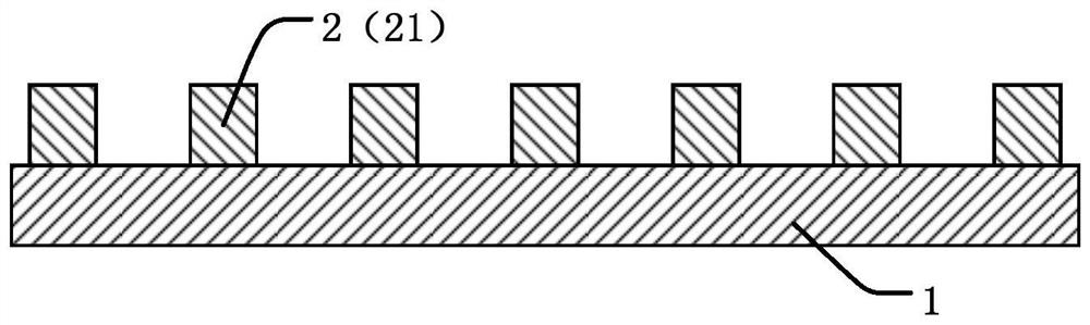
[0035] like figure 1 As shown, the embodiment of the present invention provides a display panel, including: a substrate 1 and a perovskite light-emitting film layer 2 .
[0036] The substrate 1 can be an array substrate, which plays a role of controlling the circuit switch in the display panel, and will not be described in detail here.
[0037] The perovskite light-emitting film layer 2 is arranged on the upper surface of the substrate 1, and the perovskite light-emitting film layer 2 plays the role of emitting light. The material of the perovskite light-emitting film layer 2 is mainly perovskite, and the perovskite includes zero Any of three-dimensional perovskite (0D), one-dimensional perovskite (1D), two-dimensional perovskite (2D), quasi-two-dimensional perovskite (2D), and three-dimensional perovskite (3D).
[0038] The perovskite light-emitting film layer 2 includes a perovskite light-emitting base layer 21. The perovskite light-emitting base layer 21 has a plurality of...
Embodiment 2
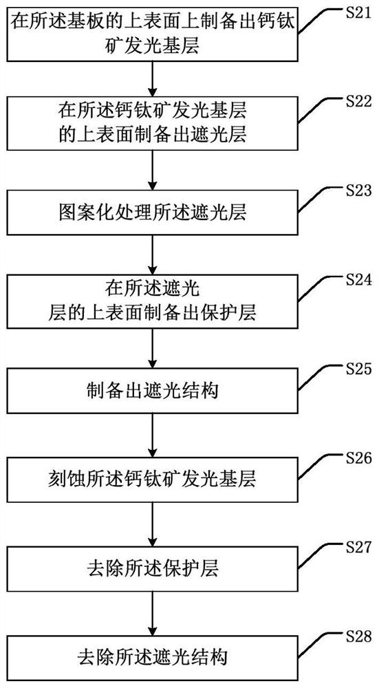
[0053] like Image 6 As shown, this embodiment provides a display panel, specifically, including: a substrate 1 and a perovskite light-emitting film layer 2 .
[0054] The substrate 1 can be an array substrate, which plays a role of controlling the circuit switch in the display panel, and will not be described in detail here.
[0055] The perovskite light-emitting film layer 2 is disposed on the upper surface of the substrate 1 , the perovskite light-emitting film layer 2 plays a role of light emission, and the perovskite light-emitting film layer 2 includes a perovskite light-emitting base layer 21 and a light-shielding structure 23 .
[0056] The material of the perovskite light-emitting base layer 21 is mainly perovskite, and the perovskite includes zero-dimensional perovskite (0D), one-dimensional perovskite (1D), two-dimensional perovskite (2D), and quasi-two-dimensional perovskite. Any of perovskite (2D) and three-dimensional perovskite (3D).
[0057] The light-shieldi...
PUM
 Abstract
Description
Claims
Application Information