Shielding structure of electronic device and manufacturing method thereof

A technology of shielding structure and electronic device, which is applied in the fields of magnetic field/electric field shielding, electrical components, etc., can solve the problems of difficulty in making electromagnetic shielding metal covers, reduced economic benefits and industrial utilization, and inability to apply to production lines for rapid production.

Inactive Publication Date: 2009-02-25
AZUREWAVE TEHNOLOGIES INC
View PDF0 Cites 7 Cited by
  • Summary
  • Abstract
  • Description
  • Claims
  • Application Information

AI Technical Summary

Problems solved by technology

[0003] Existing wireless modules or other circuit modules that require electromagnetic shielding need to be designed with an electromagnetic shielding structure such as an electromagnetic shielding metal cover according to the application requirements, and the size of the electromagnetic shielding structure must match different modules so that the circuit Isolation and isolation of the signal source in the circuit, but this kind of existing electromagnetic shielding metal cover must be designed and manufactured for different modules or devices, so that the existing electromagnetic shielding metal cover needs to consume more man-hours, manpower and cost
[0004] In addition, another disadvantage of the above-mentioned existing electromagnetic shielding metal cover is that the size, shape, and block of the electronic circuit or device that needs to be electromagnetic shielded are different. Manufacture of manual molds, stamping processing, and step-by-step component packaging make the production of electromagnetic shielding metal covers difficult and cannot be applied to rapid production lines, which reduces the economic benefits and industrial utilization of existing electromagnetic shielding metal covers.

Method used


Image

  • Shielding structure of electronic device and manufacturing method thereof
  • Shielding structure of electronic device and manufacturing method thereof
  • Shielding structure of electronic device and manufacturing method thereof

Examples


Embodiment Construction

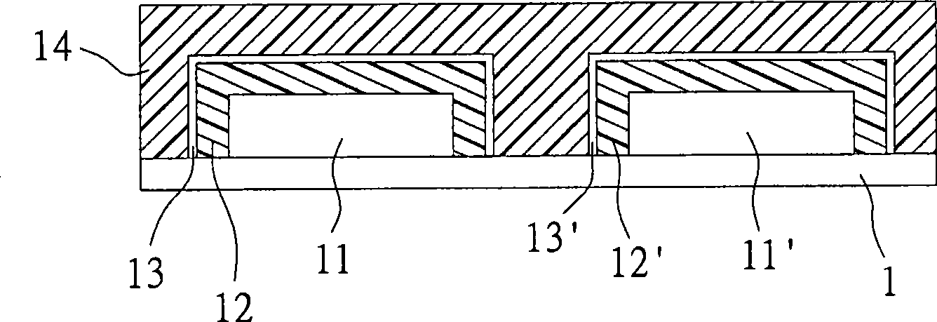
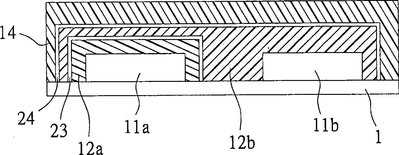
[0024] see figure 1 The present invention provides a shielding structure of an electronic device, which can effectively prevent high-frequency signals from interfering with each other.

[0025] The shielding structure of this electronic device comprises a circuit board 1, and this circuit board 1 is the circuit board that a BT resin (Bismaleimide Triazine Resin) is made in this embodiment, and this circuit board 1 has a front side and a side opposite to this front side. the underside. The circuit substrate 1 is provided with a plurality of connecting wires, including grounding terminals and other electrical circuits. The connecting wires are made by common existing methods, and will not be elaborated here.

[0026] In addition, at least one functional module 11 is disposed on one side of the circuit substrate 1 , and the functional module 11 is electrically connected to the above-mentioned connection line to achieve signal transmission. In the present embodiment, two functio...


PUM


Abstract

The invention relates to a shield structure of an electronic device, which includes: a circuit substrate; at least one function module, which is equipped on one side of the circuit substrate and is electrically connected on the circuit substrate; at least one first coating module layer, which is combined outside the function module; at least one shield layer, which is combined outside the first coating module layer; and one second coating module layer, which is combined outside the shield layer. Wherein, the shield layer is formed outside the first coating module layer by the spray finishing, printing and other modes for realizing the effect of electromagnetic shielding, thereby the shield layer can effectively reduce the production time and cost.

Description

technical field [0001] The invention relates to a shielding structure of an electronic device, in particular to a structure capable of improving electromagnetic shielding, and a manufacturing method of the shielding structure. Background technique [0002] With the development of radio frequency communication technology, it means that the circuit design of wireless communication components must be more rigorous and performance optimized. Most wireless communication products require features such as light weight, small size, high quality, low price, low power consumption, and high reliability. These features promote the technology development and market growth of RF / microwave integrated circuits. The electromagnetic shielding function and quality requirements of wireless modules in wireless communication products are relatively important to ensure that signals will not interfere with each other and affect communication quality. [0003] Existing wireless modules or other cir...

Claims


Application Information

Patent Timeline
Patent Type & Authority Applications(China)
IPC IPC(8): H05K9/00
Inventor 黄忠谔黄建渝
Owner AZUREWAVE TEHNOLOGIES INC
Why Eureka
Try Eureka