Sub-wave length embedded type grating structure polarizing sheet and manufacturing method thereof
A grating structure, embedded technology, used in polarizing elements, microlithography exposure equipment, photolithography process exposure devices, etc., can solve the problems of inability to use industrial applications, low production efficiency, small area, etc. Transmission efficiency, simple manufacturing process, and the effect of protecting the metal layer
- Summary
- Abstract
- Description
- Claims
- Application Information
AI Technical Summary
Problems solved by technology
Method used
Image
Examples
Embodiment 1
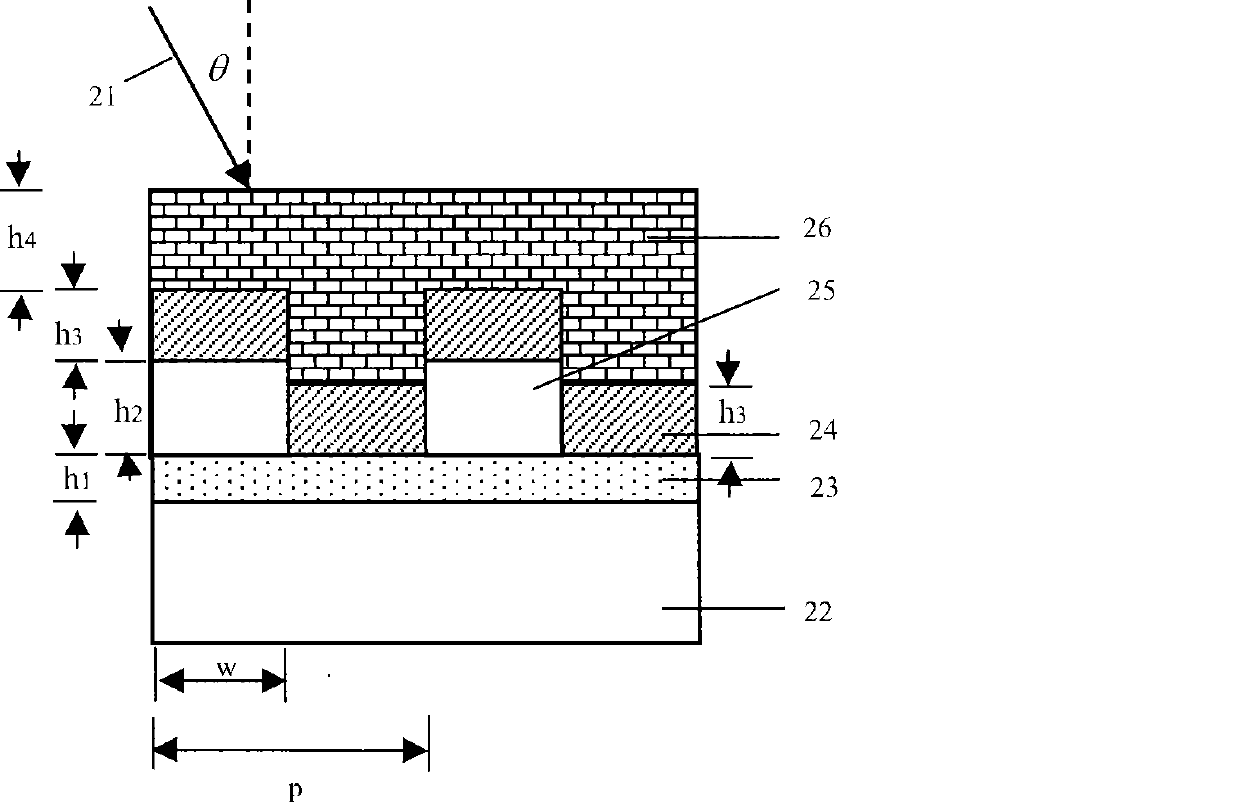
[0041] See attached figure 2 , is a schematic diagram of a subwavelength embedded grating structure polarizer.
[0042] The transparent substrate 22 is made of glass or plastic film with a thickness of 12-150um. The plastic can be polycarbonate (PC), polyvinyl chloride (PVC), polyester (PET), polymethylmethacrylate (PMMA) or polypropylene (BOPP).
[0043] The refractive index of the high refractive index medium layer 23 is greater than that of the substrate.
[0044] High refractive index medium layer 23 can be TiO 2 、 Ta 2 o 5 , ZnS and so on.
[0045] The metal layer 24 can be a gold, silver, copper, aluminum layer.
[0046]The dielectric grating 25 is made of plastic, which can be polycarbonate (PC), polyvinyl chloride (PVC), polyester (PET), polymethyl methacrylate (PMMA) or polypropylene (BOPP).
[0047] The cover layer 26 may be CaF 2 Or plastic or resin coating.
[0048] Wherein, the period p of the dielectric grating is less than or equal to 250nm;
[0049] ...
Embodiment 2
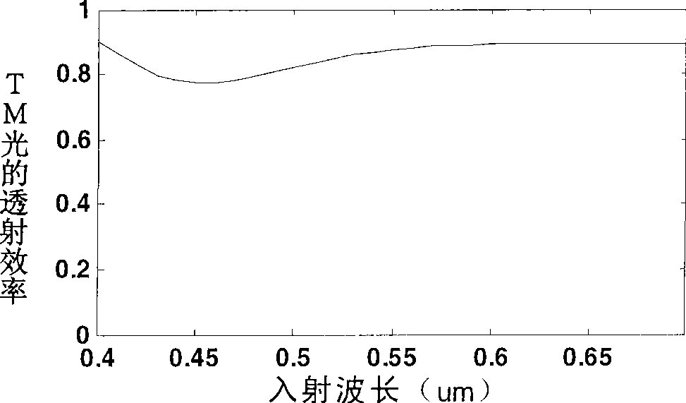
[0059] see figure 2 , changing the refractive index of the high refractive index medium layer, the refractive index of the dielectric covering layer, and the height of the metal layer in Embodiment 1. The refractive index of the high refractive index medium layer 23 is 2.2, the dielectric covering layer 26 is CaF2 with a refractive index of 1.4, and the height h3 of the metal layer is 0.07um. The incident light 21 is visible light with a wavelength of 400nm-700nm and an incident angle of 0 degrees; the substrate 22 is polyester film (PET) with a refractive index of 1.48; the metal layer 24 is aluminum; the dielectric grating 25 is PMMA with a refractive index of 1.48. Other structural parameters of the polarizer are as follows: the thickness of the base is 1000um, the thickness h1 of the high refractive index medium layer is 0.05um, the height of the dielectric grating h2=0.1um, the thickness of the dielectric covering layer h4=0.1um, and the period of the dielectric grating ...
Embodiment 3
[0062] The thickness h4 of the dielectric covering layer in Embodiment 1 is changed, and other parameters remain unchanged. When the incident wavelength is 400nm, the influence of the thickness h4 of the dielectric covering layer on the transmission efficiency and extinction ratio of TM light is as follows: Figure 5 , Image 6 shown. With the increase of h4, the transmission efficiency of TM light changes periodically in the range of 87.0%-91.6%, and the extinction ratio changes periodically in the range of 4.0E4-10.0E4. It can be seen that the dielectric covering layer can modulate the transmission efficiency of the polarizer.
[0063] Considering that the thickness of the dielectric cover layer is too thick, the thickness of the polarizer will be increased, thereby increasing the difficulty of integrating the polarizer with other optical devices. Generally, the thickness of the dielectric cover layer corresponding to the first peak of the transmission efficiency of TM lig...
PUM
| Property | Measurement | Unit |
|---|---|---|
| thickness | aaaaa | aaaaa |
| thickness | aaaaa | aaaaa |
| angle of incidence | aaaaa | aaaaa |
Abstract
Description
Claims
Application Information
 - R&D
- Intellectual Property
- Life Sciences
- Materials
- Tech Scout
- Unparalleled Data Quality
- Higher Quality Content
- 60% Fewer Hallucinations
Browse by: Latest US Patents, China's latest patents, Technical Efficacy Thesaurus, Application Domain, Technology Topic, Popular Technical Reports.
© 2025 PatSnap. All rights reserved.Legal|Privacy policy|Modern Slavery Act Transparency Statement|Sitemap|About US| Contact US: help@patsnap.com


