Modified capacitor and method for manufacturing same

A manufacturing method and improved technology, applied in semiconductor/solid-state device manufacturing, circuits, electrical components, etc., can solve problems such as increasing the difficulty of device manufacturing, increasing the size of semiconductor devices, and affecting the area of ​​pixel arrays

Inactive Publication Date: 2010-08-25
SEMICON MFG INT (SHANGHAI) CORP
View PDF0 Cites 0 Cited by
  • Summary
  • Abstract
  • Description
  • Claims
  • Application Information

AI Technical Summary

Problems solved by technology

Capacitors used in current semiconductor devices usually adopt a metal / dielectric / metal (Metal / dielectric / metal) structure, which usually uses the metal layer inside the device as the lower electrode of the capacitor, and then deposits an insulating dielectric on the lower electrode layer and metal layer, and then photolithography and etching according to the capacitor pattern to obtain the insulating dielectric layer and the upper electrode of the capacitor, but in order to facilitate the electrical connection of other devices with the capacitor, it is necessary to manufacture another layer on the upper electrode. The metal layer used for connecting other devices to the capacitor will increase the size of semiconductor devices, and may also increase the difficulty of manufacturing some devices, hindering their development in the direction of miniaturization
[0003] In order to overcome the various problems caused by capacitors with MIM structures, the industry has proposed a capacitor with a polysilicon / insulating dielectric layer / polysilicon (Poly / dielectric / Poly) structure. The upper and lower electrodes of the capacitor are polysilicon. The polysilicon of the electrode is usually formed together when the MOS transistor is multi-passed by the silicon gate, and then an insulating dielectric layer and polysilicon are deposited on the lower electrode, and then photolithography and etching are performed according to the capacitance pattern to obtain the insulating dielectric layer and the capacitance of the capacitor. Polysilicon upper electrode, the use of capacitors with this structure will reduce the thickness of the semiconductor device, but it will affect the area of ​​other functional parts of the semiconductor device because this capacitor is manufactured in the metal pre-dielectric, for example, in CMOS image sensors, it will affect Area of ​​Pixel Array

Method used


Image

  • Modified capacitor and method for manufacturing same
  • Modified capacitor and method for manufacturing same
  • Modified capacitor and method for manufacturing same

Examples


Embodiment Construction

[0020] The improved capacitor of the present invention and its manufacturing method will be further described in detail below.

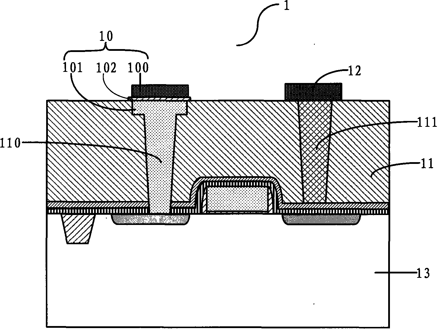
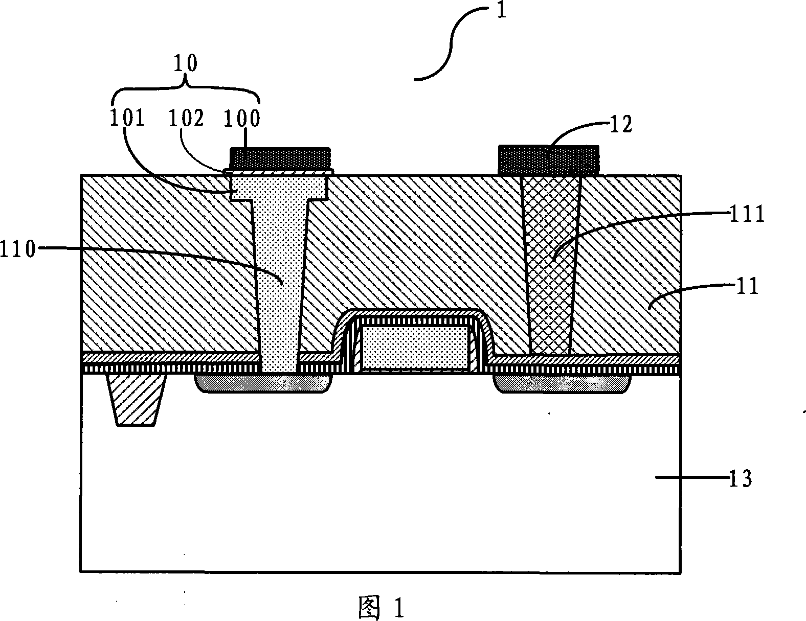
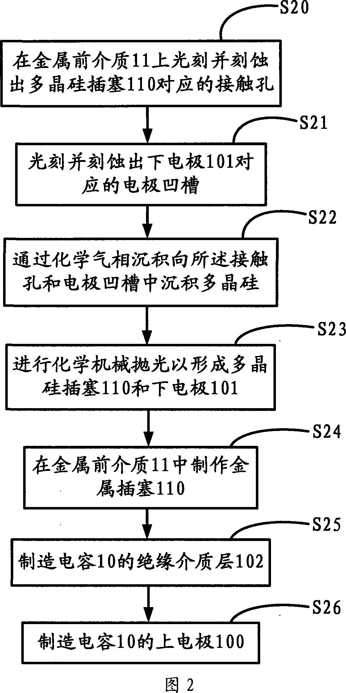
[0021] Referring to FIG. 1, the improved capacitor 10 of the present invention is arranged in a semiconductor device 1 that has fabricated a pre-metal dielectric 11 and a first metal layer 12, and the pre-metal dielectric 11 is provided with connected electrode grooves and contacts holes (not shown), and the cross-sectional area of ​​the electrode groove is larger than the maximum cross-sectional area of ​​the contact hole. The capacitor 10 includes upper and lower electrodes 100, 101 and an insulating medium layer 102 sandwiched between the upper and lower electrodes 100, 101, the upper electrode 100 is arranged in the first metal layer 12, and the lower electrode 101 is arranged in the first metal layer 12. The bottom electrode 101 is also connected to the silicon substrate 13 of the semiconductor device 1 through the polysilicon plug 110 disposed ...


PUM


Abstract

The invention provides an improved capacitor and a manufacturing method thereof. The capacitor which adopts an MIM structure or a PIP structure in the prior art has the problems of large storage space, and the like, thereby not being capable of complying with the development demands of miniaturization of semiconductor devices. The capacitor is arranged in a semiconductor device with a pre-metal dielectric and a first metal layer which are manufactured, an electrode groove and a contact hole which are communicated are arranged in the pre-metal dielectric, the capacitor comprises upper and lower electrodes and an insulating dielectric layer which is clamped and arranged between the two electrodes, the lower electrode is made of polysilicon and is arranged in the electrode groove, the lower electrode is connected to a silicon substrate of the semiconductor device through a polysilicon plug which is arranged in the contact hole, and the upper electrode is arranged in the first metal layer. The manufacturing method of the capacitor firstly photoengraves and etches the contact hole and the electrode groove, then the polysilicon is deposited, then the chemical mechanical polishing is carried out to form the polysilicon plug and the lower electrode and finally, the insulating dielectric layer and the upper electrode are manufactured. The development demands of the miniaturization of the semiconductor devices can be complied by the capacitor and the manufacturing method.

Description

technical field [0001] The invention relates to a capacitor device, in particular to an improved capacitor and a manufacturing method thereof. Background technique [0002] In order to meet the needs of portable electronic products, semiconductor devices used in electronic products are also developing towards miniaturization. In the process of miniaturization of semiconductor devices, in addition to continuously reducing the volume of MOS transistors, the reduction of capacitor volume in some semiconductor devices with integrated capacitors (such as CMOS image sensors) has also become the focus of research on the miniaturization of semiconductor devices. Capacitors used in current semiconductor devices usually adopt a metal / dielectric / metal (Metal / dielectric / metal) structure, which usually uses the metal layer inside the device as the lower electrode of the capacitor, and then deposits an insulating dielectric on the lower electrode layer and metal layer, and then photolith...

Claims


Application Information

Patent Timeline
Patent Type & Authority Patents(China)
IPC IPC(8): H01L27/04H01L27/146H01L21/822
Inventor 杨承罗飞王娉婷朱虹
Owner SEMICON MFG INT (SHANGHAI) CORP
Why Eureka
Try Eureka