Nanowire transistor with surrounding gate

A transistor, surround gate technology, applied in transistors, nanotechnology for information processing, nanotechnology, etc., can solve problems such as difficult structure realization

Active Publication Date: 2009-04-15
MICRON TECH INC
View PDF0 Cites 11 Cited by
  • Summary
  • Abstract
  • Description
  • Claims
  • Application Information

AI Technical Summary

Problems solved by technology

Surrounding gate structures provide desirable control over the transistor channel, but are difficult to achieve in practice

Method used


Image

  • Nanowire transistor with surrounding gate
  • Nanowire transistor with surrounding gate
  • Nanowire transistor with surrounding gate

Examples


Embodiment Construction

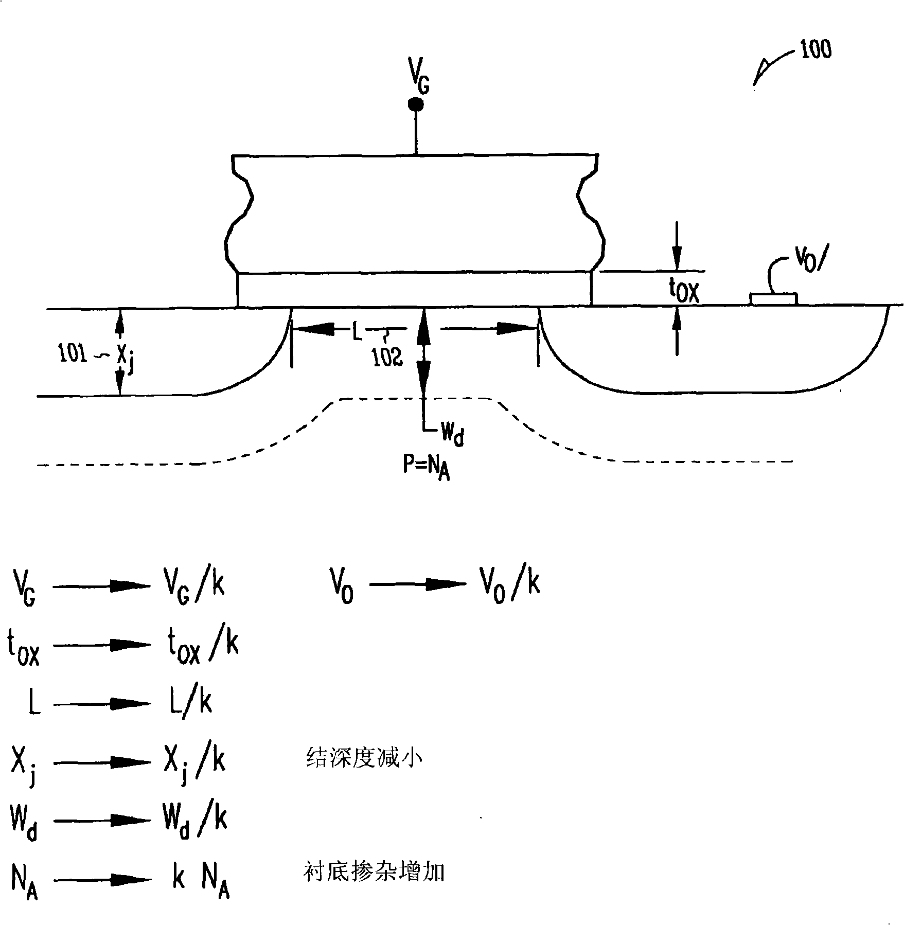
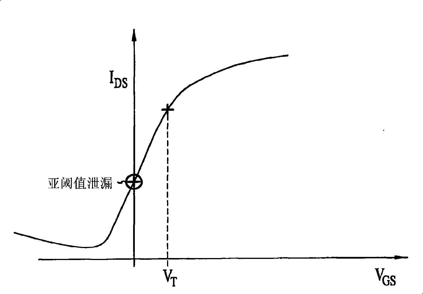
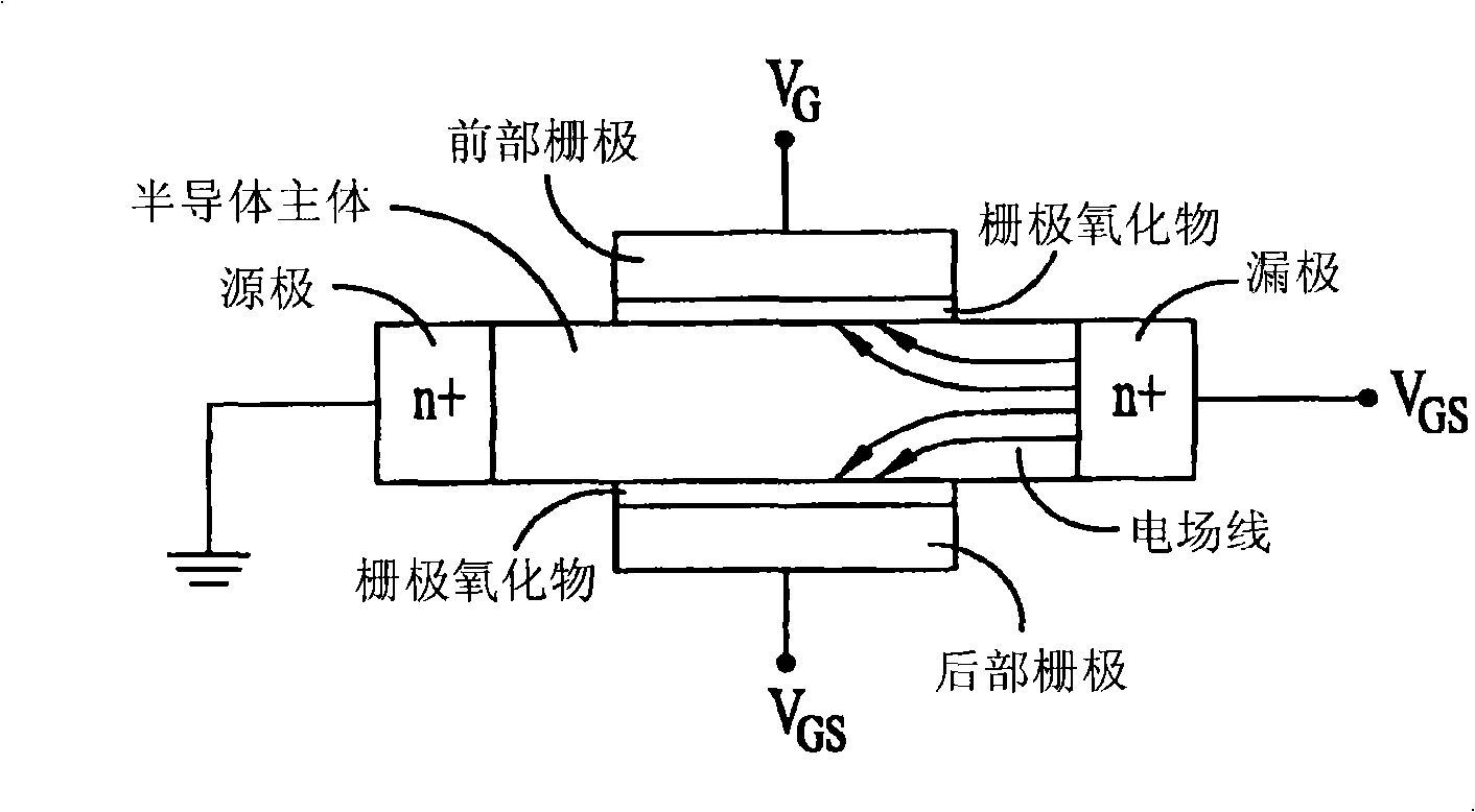
[0024] The following detailed description refers to the accompanying drawings, which show, by way of illustration, specific aspects and embodiments in which the inventive subject matter may be practiced. These embodiments are described in sufficient detail to enable those skilled in the art to practice the inventive subject matter. The various embodiments of the inventive subject matter are not necessarily mutually exclusive, as aspects of one embodiment may be combined with aspects of another embodiment. Other embodiments may be utilized and structural, logical, and electrical changes may be made without departing from the scope of the inventive subject matter. In the following description, the terms "wafer" and "substrate" are used interchangeably to refer generally to any structure on which integrated circuits are formed, and also to refer to such structures during the various stages of integrated circuit fabrication. Both terms include doped and undoped semiconductors, ep...


PUM


Abstract

One aspect of the present subject matter relates to a method for forming a transistor. According to an embodiment of the method, a pillar of amorphous semiconductor material is formed on a crystalline substrate, and a solid phase epitaxy process is performed to crystallize the amorphous semiconductor material using the crystalline substrate to seed the crystalline growth. The pillar has a sublithographic thickness. A transistor body is formed in the crystallized semiconductor pillar between a first source/drain region and a second source/drain region. A surrounding gate insulator is formed around the semiconductor pillar, and a surrounding gate is formed around and separated from the semiconductor pillar by the surrounding gate insulator. Other aspects are provided herein.

Description

[0001] Cross References to Related Applications [0002] This document claims priority to the following applications: U.S. Application Serial No. 11 / 397,430, filed April 4, 2006, entitled "Grown Nanofin Transistors"; U.S. Application No. 11 / 397,358, entitled "Etched Nanofin Transistors"; 11 filed April 4, 2006, entitled "DRAM With Nanofin Transistors" / 397,413 U.S. Application; and U.S. Application No. 11 / 397,406, entitled "Tunneling Transistor with Sublithographic Channel," filed April 4, 2006, each of which is incorporated by reference into this article. technical field [0003] The present invention relates generally to semiconductor devices, and more particularly to nanowire transistors with surrounding gates. Background technique [0004] The semiconductor industry has a market-driven need to reduce the size of devices, such as transistors, and to increase device density on substrates. Some product goals include lower power consumption, higher performance and smalle...

Claims


Application Information

Patent Timeline
Patent Type & Authority Applications(China)
IPC IPC(8): H01L21/336H01L29/06H01L29/786H01L21/8242H01L21/20
CPCY10S977/932H01L29/0676Y10S977/762H01L29/0665B82Y10/00Y10S977/70H01L29/7827Y10S977/936H01L29/0673H01L29/66666
Inventor 伦纳德·福布斯
Owner MICRON TECH INC
Why Eureka
Try Eureka