Surface flaw detecting method and device
A technology of surface flaws and detection methods, which is applied in the direction of optical testing flaws/defects, image enhancement, instruments, etc., can solve the problem of not being able to determine whether the detected object has flaws, etc., and achieve the effect of avoiding interference from human factors and improving accuracy
- Summary
- Abstract
- Description
- Claims
- Application Information
AI Technical Summary
Problems solved by technology
Method used
Image
Examples
Embodiment Construction
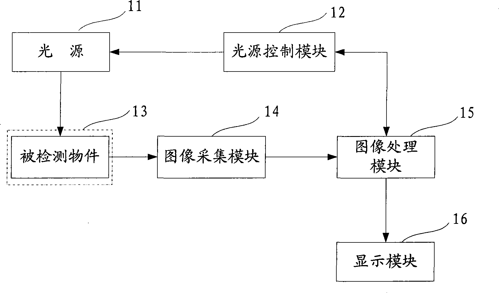
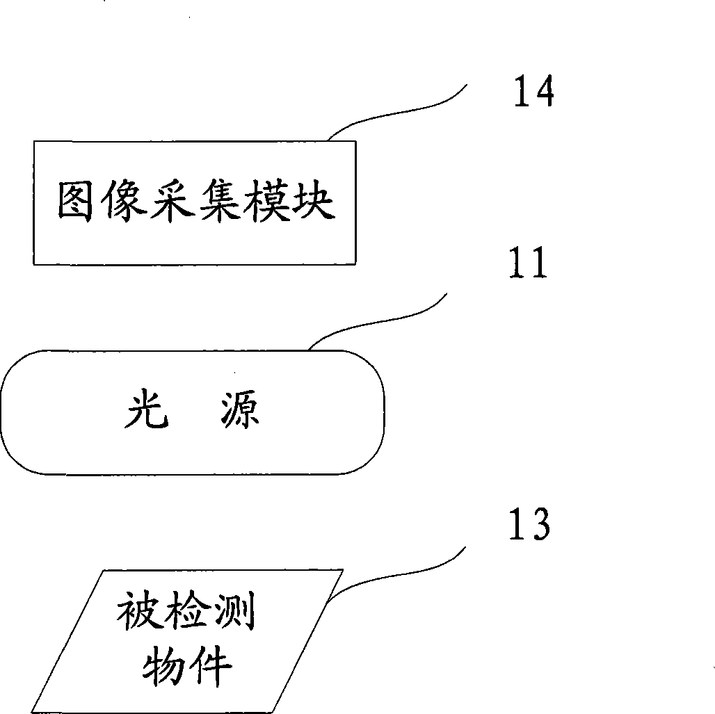
[0015] refer to figure 1 , shows a schematic diagram of a defect detection device, which includes a light source 11, a light source control module 12, an image acquisition module 14, an image processing module 15, and a display module 16, wherein the image processing module 15 is connected to the image acquisition module 14 and the display module respectively. The module 16 is connected to the light source control module 12 , and the light source 11 is connected to the light source control module 12 . Such as figure 2 As shown, during image acquisition, the detected object 13 is placed between the image acquisition module 14 and the light source 11 .
[0016] The light source 11 can provide uniform brightness for the detected object. In this embodiment, the ring-shaped purple light source is preferred.
[0017] The light source control module 12 executes the light source control action through the instruction issued by the image processing module 15, and adjusts the bright...
PUM
 Abstract
Description
Claims
Application Information


